Method of manufacturing nonvolatile memory element, and nonvolatile memory element

a technology of nonvolatile memory elements and memory cells, which is applied in the direction of bulk negative resistance effect devices, basic electric elements, electrical equipment, etc., can solve the problems of difficult to accelerate operations, hinder low voltage operations, and difficult to change the resistance state, so as to reduce the voltage and high-density memory cells

Inactive Publication Date: 2013-04-04
PANASONIC INTELLECTUAL PROPERTY MANAGEMENT CO LTD
View PDF7 Cites 10 Cited by
  • Summary
  • Abstract
  • Description
  • Claims
  • Application Information

AI Technical Summary

Benefits of technology

[0030]According to the present invention, a method of manufacturing a variable resistance nonvolatile memory element capable of reducing a voltage upon initial breakdown can be provided. Even when a load resistor is connected to a variable resistance nonvolatile memory element such as a variable resistance element, there is no need to increase a voltage for an initial breakdown step, so that a high-density memory cell array can be realized without an increase in size of a transistor and the like.

Problems solved by technology

To change the variable resistance material from the low resistance state to the high resistance state, however, a long pulse of the order of microseconds is needed, which makes it difficult to accelerate operations.
Besides, in the unipolar type element, the resistance state is hard to be changed immediately after the structure in which the variable resistance layer is placed between the upper and lower electrodes is formed.
This hinders low voltage operations.

Method used


Image

  • Method of manufacturing nonvolatile memory element, and nonvolatile memory element
  • Method of manufacturing nonvolatile memory element, and nonvolatile memory element
  • Method of manufacturing nonvolatile memory element, and nonvolatile memory element

Examples


experiment 1

(Experiment 1)

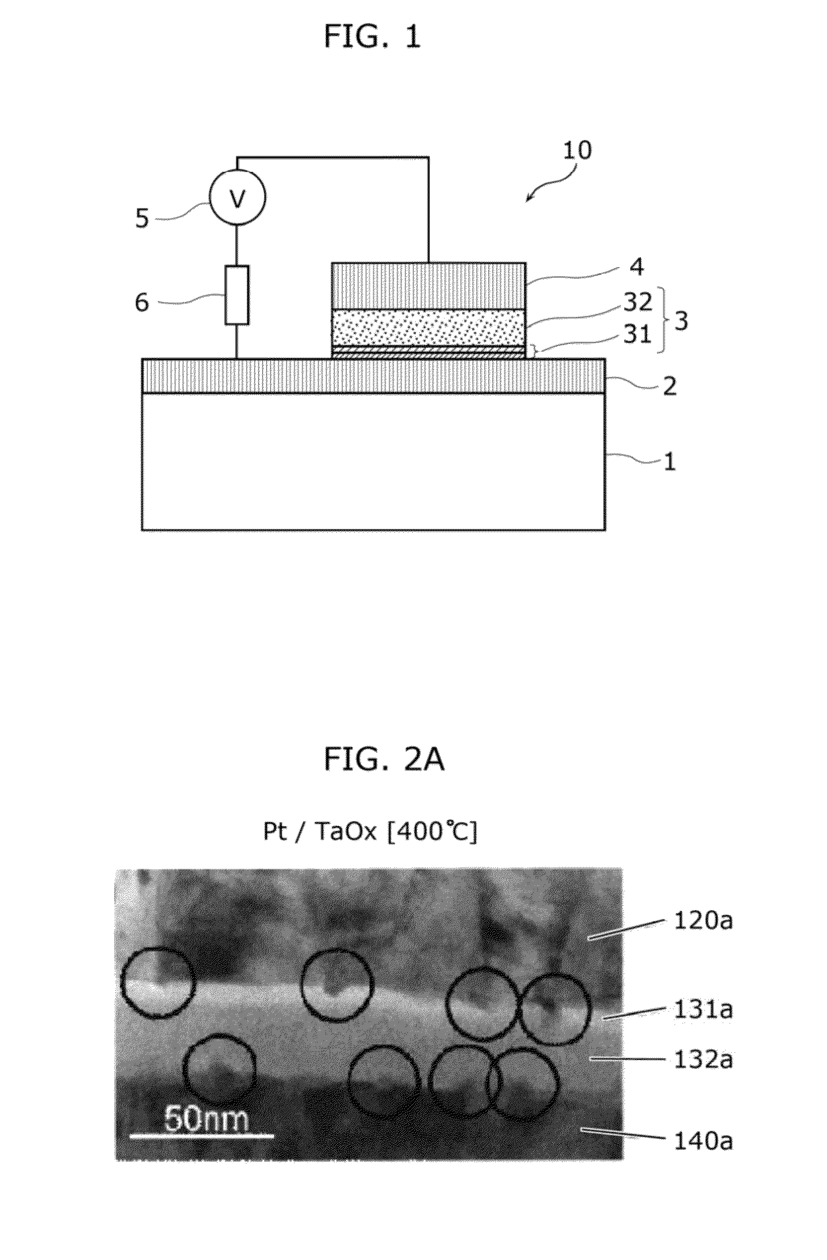
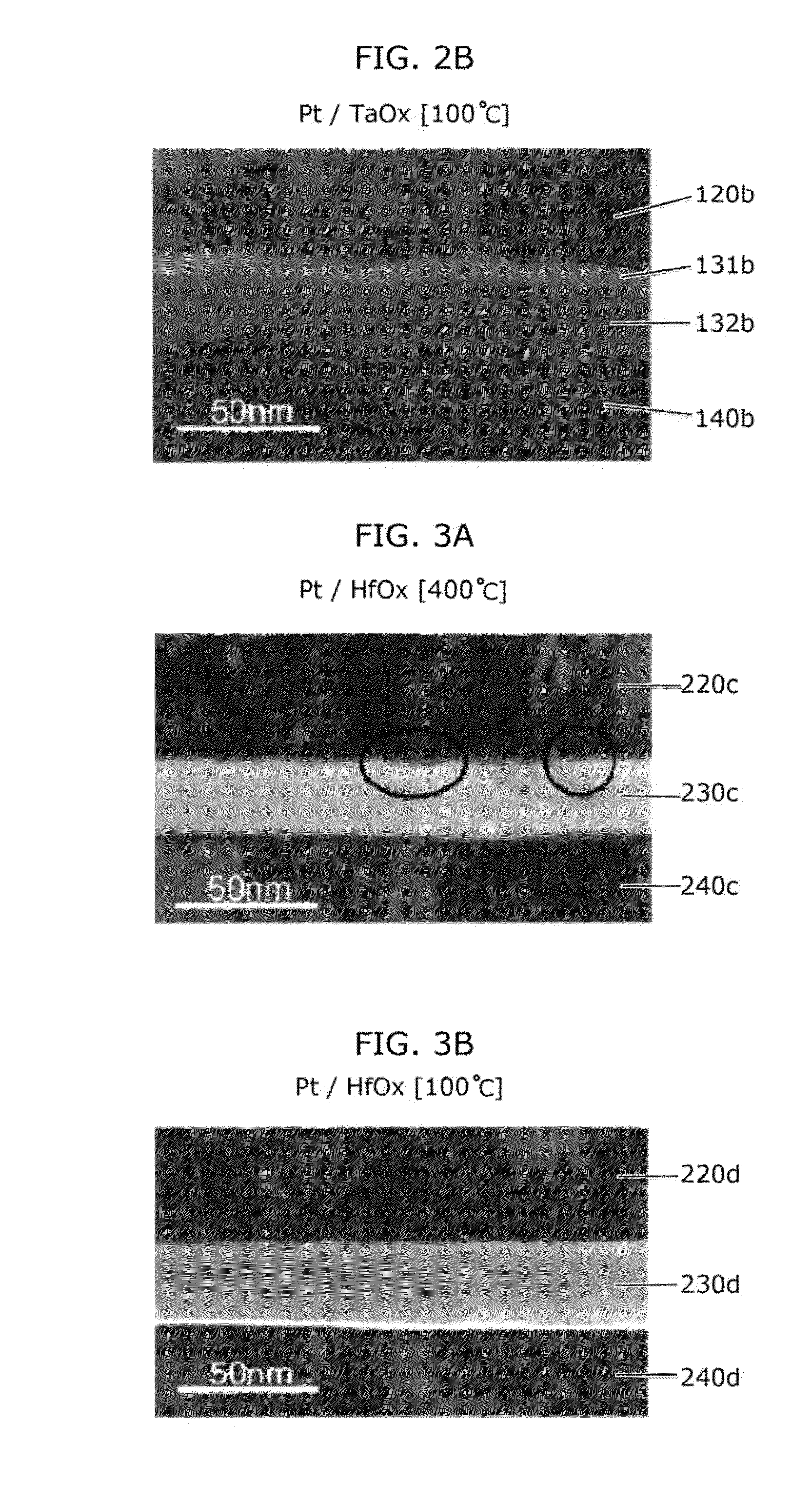
[0089]FIGS. 2A and 2B are each a transmission electron microscope (TEM) photograph showing a cross section of a nonvolatile memory element in which oxygen-deficient tantalum oxide is used in the variable resistance layer and Pt is used in the electrodes. FIG. 2A corresponds to the case where 400° C. is the maximum temperature in the process, and FIG. 2B corresponds to the case where 100° C. is the maximum temperature in the process.

[0090]In the element shown in FIG. 2A, a second oxygen-deficient tantalum oxide layer 132a of about 23 nm in film thickness, a first oxygen-deficient tantalum oxide layer 131a of about 8 nm in film thickness, and a first electrode layer 120a comprising a Pt layer of about 80 nm in film thickness are stacked in this order on a second electrode layer 140a comprising a Pt layer of about 50 nm in film thickness. The first oxygen-deficient tantalum oxide layer 131a is higher in oxygen content (substantially Ta2O5 in composition) than the second o...

experiment 2

(Experiment 2)

[0101]The inventors of the present invention then examined whether or not the same problem arises in the case of using hafnium instead of tantalum as the transition metal included in the variable resistance layer.

[0102]FIGS. 3A and 3B are each a transmission electron microscope (TEM) photograph showing a cross section of a nonvolatile memory element in which oxygen-deficient hafnium oxide is used in the variable resistance layer. FIG. 3A corresponds to the case where 400° C. is the maximum temperature in the process, and FIG. 33 corresponds to the case where 100° C. is the maximum temperature in the process.

[0103]In the element shown in FIG. 3A, an oxygen-deficient hafnium oxide layer 230c of about 30 nm in film thickness and a first electrode layer 220c comprising Pt of about 75 nm in film thickness are stacked in this order on a second electrode layer 240c comprising a W (tungsten) layer of about 150 nm in film thickness. The element shown in FIG. 3A was equally prod...

experiment 3

(Experiment 3)

[0108]As a result of conducting further study based on these findings, the inventors of the present invention have found out that projections can be suppressed by reducing the film thickness of the electrode layer comprising Pt. This is described below.

[0109]FIGS. 4A to 4C are each a transmission electron microscope (TEM) photograph showing an element cross section in this example. FIG. 4A shows a cross section of an element A, FIG. 4B shows a cross section of an element B, and FIG. 4C shows a cross section of an element C.

[0110]A first electrode layer 320a comprising a Pt layer in the element A shown in FIG. 4A is 8 nm in thickness, a first electrode layer 320b comprising a Pt layer in the element B is 13 nm in thickness, and a first electrode layer 320c comprising a Pt layer in the element C is 23 nm in thickness. All of the elements have the same structure except the thickness of the Pt layer. In detail, in the element A shown in FIG. 4A, a second electrode layer 34...


PUM

PropertyMeasurementUnit
thicknessaaaaaaaaaa
thicknessaaaaaaaaaa
thicknessaaaaaaaaaa

Abstract

A variable resistance nonvolatile memory element manufacturing method includes: forming a first electrode on a substrate; forming a first metal oxide layer having a predetermined oxygen content atomic percentage on the first electrode; forming, in at least one part of the first metal oxide layer, a modified layer higher in resistance than the first metal oxide layer, by oxygen deficiency reduction; forming a second metal oxide layer lower in oxygen content atomic percentage than the first metal oxide layer, on the modified layer; and forming a second electrode on the second metal oxide layer. A variable resistance layer includes the first metal oxide layer having the modified layer and the second metal oxide layer, connects to the first electrode and the second electrode, and changes between high and low resistance states according to electrical pulse polarity.

Description

TECHNICAL FIELD[0001]The present invention relates to a method of manufacturing a variable resistance nonvolatile memory element that changes in resistance value according to an applied electrical signal.BACKGROUND ART[0002]With advances in digital technology, electronic appliances such as mobile information appliances and home information appliances are increasingly sophisticated in recent years. Such sophistication of electronic appliances is accompanied by rapid miniaturization and acceleration of semiconductor elements used. In particular, large-capacity nonvolatile memories, represented by flash memories, are finding rapidly expanding use. Moreover, nonvolatile memory devices including variable resistance nonvolatile memory elements are under research and development as new, next-generation nonvolatile memories that can replace flash memories. A variable resistance nonvolatile memory element mentioned here is such an element that has a property of reversibly changing in resista...

Claims


Application Information

Patent Timeline
Patent Type & Authority Applications(United States)
IPC IPC(8): H01L45/00
CPCH01L45/145H01L45/16H01L45/08H01L45/1625H01L45/146H01L45/1641H01L45/1675H01L45/1233H10N70/24H10N70/826H10N70/8833H10N70/041H10N70/026H10N70/063H10N70/011H10N70/883
Inventor KATAYAMA, KOJITAKAGI, TAKESHI
Owner PANASONIC INTELLECTUAL PROPERTY MANAGEMENT CO LTD
Why Eureka
Try Eureka