Semiconductor device and fabrication method of the semiconductor device

a technology of semiconductor devices and semiconductors, applied in the direction of semiconductor/solid-state device details, manufacturing tools, non-electric welding apparatus, etc., can solve the problems of compromising the reliability the inability to use the characteristics of the sic device, and the inability to drive the sic device at high temperature, so as to achieve the effect of reducing the length of the process

Active Publication Date: 2013-04-18
ROHM CO LTD
View PDF10 Cites 19 Cited by
  • Summary
  • Abstract
  • Description
  • Claims
  • Application Information

AI Technical Summary

Benefits of technology

[0019]According to the preset invention, it can provide the semiconductor device having the flip chip structure whose process temperature becomes lowered temperature and process time length also can be shortened by using the solid phase diffusion bonding, and provide the fabrication method of such semiconductor device.

Problems solved by technology

However, the SiC devices can theoretically operate in temperatures reaching about 400 degrees C. Therefore, if the SiC devices are driven at high temperature when using the conventional low melting point solder, a short circuit between electrodes, a delamination between the SiC device and a base plate, etc. will occur due to fusing of bonding parts where the low melting point solder is used, and thereby compromising reliability of the SiC devices.
Accordingly, the SiC devices could not be driven at high temperature, and therefore the characteristics of the SiC devices were not able to be used.
However, taking mass production into consideration, the bonding under the high temperature melting point is not suitable for mass productivity because a period of process time is so long.
Since process temperature is also still higher when using the bonding under the high temperature melting point, an excessive stress is applied to materials due to the difference in a coefficient of thermal expansion between individual materials used for fabricating a module, and thereby it cannot secure the reliability of the SiC devices.

Method used


Image

  • Semiconductor device and fabrication method of the semiconductor device
  • Semiconductor device and fabrication method of the semiconductor device
  • Semiconductor device and fabrication method of the semiconductor device

Examples


embodiment

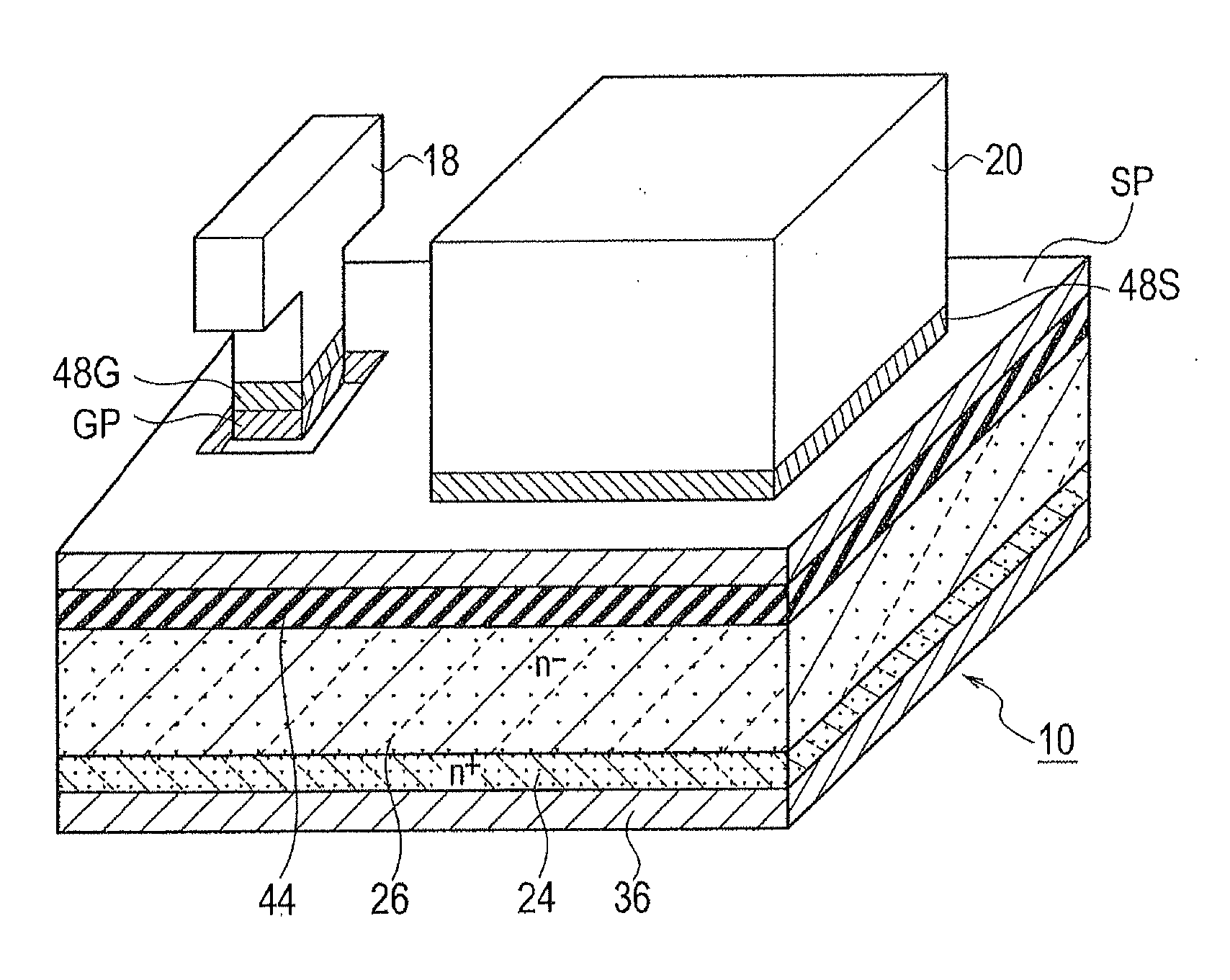
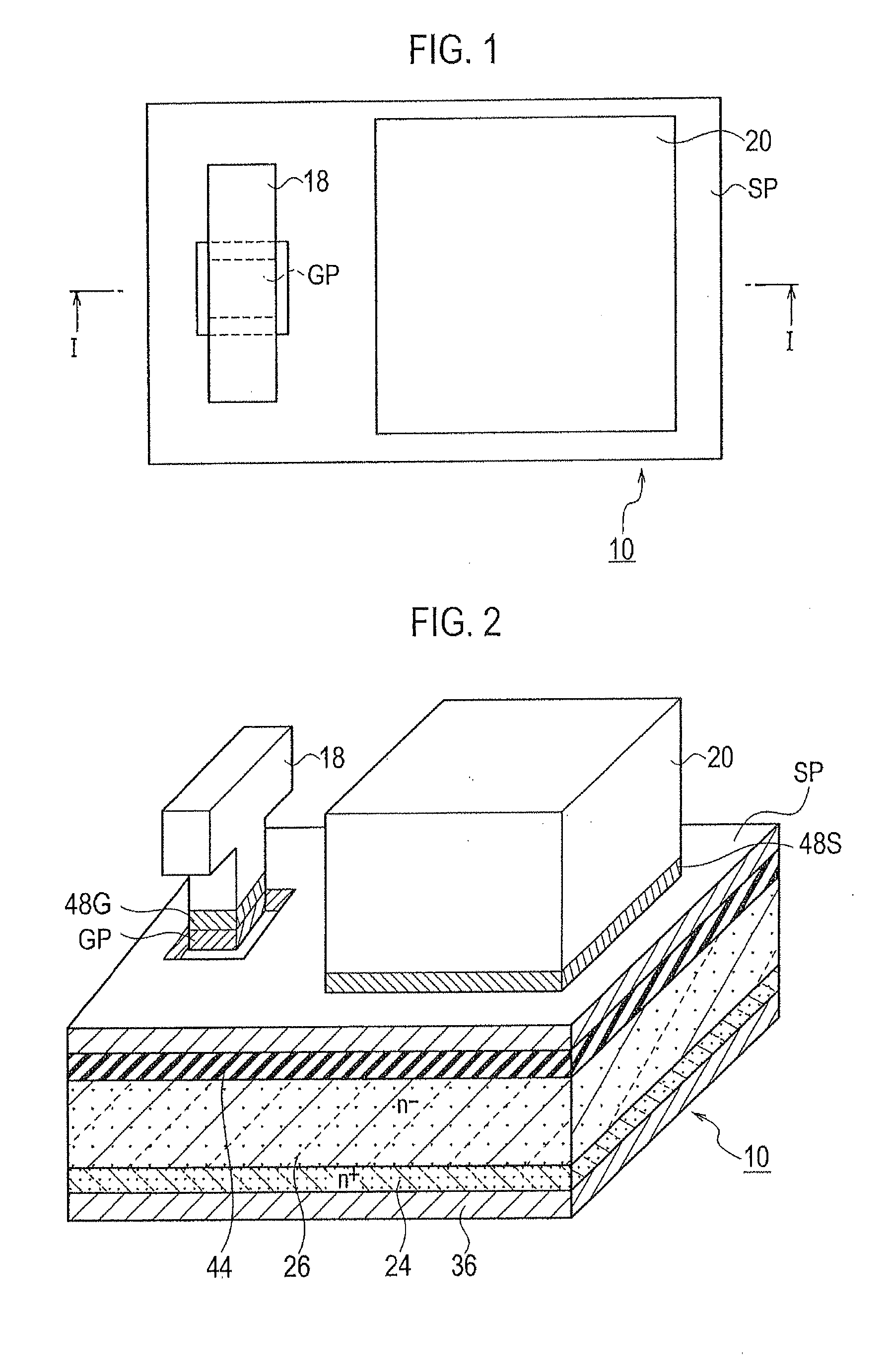
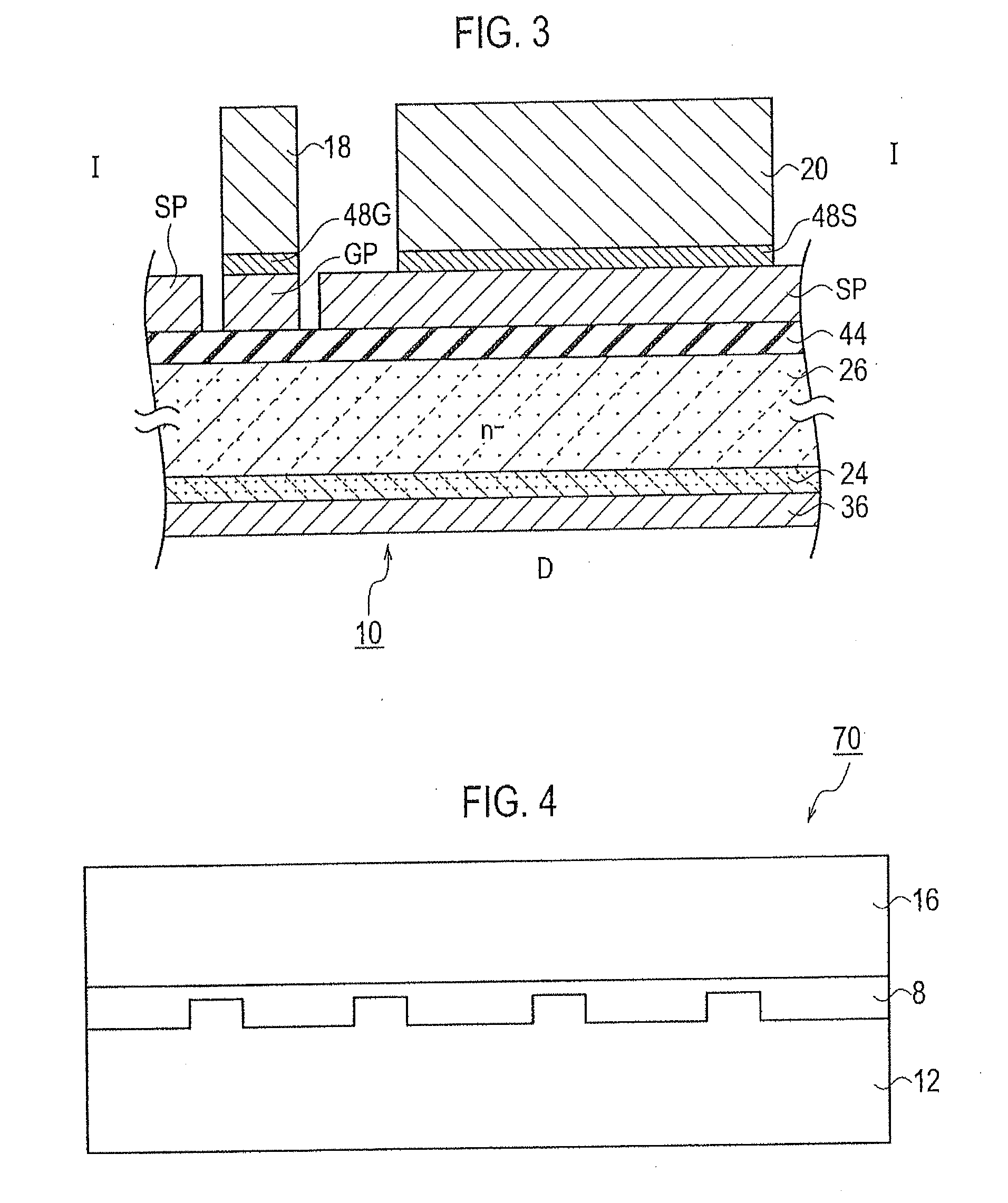
[0047]A schematic planar pattern configuration of a semiconductor chip (e.g., a power transistor) 10 mounted in a semiconductor device 1 according to a embodiment is represented as shown in FIG. 2, a schematic bird's-eye view structure of the semiconductor chip 10 is represented as shown in FIG. 2, and a schematic cross-sectional configuration taken in the line I-I of FIG. 1 is represented as shown in FIG. 3.

[0048]As shown in FIG. 1 to FIG. 3, the semiconductor chip 10 mounted in the semiconductor device 1 according to the embodiment includes: a semiconductor substrate 26; a gate pad electrode GP and a source pad electrode SP are disposed on an interlayer insulating film 44 formed on a surface of the semiconductor substrate 26; a gate connector 18 disposed on the gate pad electrode GP via an gate solid phase diffusion bonding layer 48G; a source connector 20 disposed on the source pad electrode SP via a source solid phase diffusion bonding layer 48S; and a drain pad electrode 36 dis...

modified example 1

[0067]FIG. 9A shows a schematic bird's-eye view configuration diagram showing a semiconductor device 1 according to a modified example 1 of the embodiment, and FIG. 9B shows a schematic cross-sectional configuration diagram taken in the line of FIG. 9A. In the semiconductor device 1 according to the modified example 1 of the embodiment, a plurality of the semiconductor chips 101, 102 and 103 are respectively disposed in flip chip configuration toward the signal wiring electrodes 12 and the power wiring electrodes 16 disposed on the insulating substrate 8, and the drain connector DC is disposed in common on the drain pad electrodes 361, 362 and 363. In the semiconductor device 1 according to the modified example 1 of the embodiment, the respective gate pad electrodes GP and the respective source pad electrodes SP are disposed in parallel, and the gate connectors 181, 182, and 183 disposed on the respective gate pad electrodes GP and the source connectors 201, 202 and 203 disposed on ...

modified example 2

[0070]As shown in FIG. 10, a semiconductor device 1 according to a modified example 2 of the embodiment includes: an insulating substrate 8; a signal wiring electrode 12 disposed on the insulating substrate 8; a power wiring electrode 16a disposed so as to pass through the insulating substrate 8; a semiconductor chip 101 disposed in flip chip configuration on the insulating substrate 8 and including a semiconductor substrate 26, a source pad electrode SP and a gate pad electrode GP disposed on a surface of the semiconductor substrate 26, and a drain pad electrodes 361 disposed on a back side surface of the semiconductor substrate 26; a gate connector 181 disposed on the gate pad electrode GP; and a source connector 201 disposed on the source pad electrode SP. In this case, between the gate connector 181 and the gate pad electrode GP, and between the gate connector 181 and the signal wiring electrode 12 are bonded by using solid phase diffusion bonding. Similarly, between the source ...


PUM

PropertyMeasurementUnit
bandgap energyaaaaaaaaaa
pressureaaaaaaaaaa
pressureaaaaaaaaaa

Abstract

The semiconductor device having flip chip structure includes: an insulating substrate; a signal wiring electrode disposed on the insulating substrate; a power wiring electrode disposed on the insulating substrate or disposed so as to pass through the insulating substrate; a semiconductor chip disposed in flip chip configuration on the insulating substrate and comprising a semiconductor substrate, a source pad electrode and a gate pad electrode disposed on a surface of the semiconductor substrate, and a drain pad electrode disposed on a back side surface of the semiconductor substrate; agate connector disposed on the gate pad electrode; and a source connector disposed on the source pad electrode. The gate connector, the gate pad electrode and the signal wiring electrode are bonded, and the source connector, the source pad electrode and the power wiring electrode are bonded, by using solid phase diffusion bonding.

Description

TECHNICAL FIELD[0001]The present invention relates to a semiconductor device and a fabrication method of such semiconductor device. In particular, the present invention relates to a semiconductor device having a flip chip structure by solid phase diffusion bonding, and a fabrication method of such semiconductor device.BACKGROUND ART[0002]Recently, research is conducted to develop Silicon Carbide (SiC) devices in many research institutions. As characteristics of the SiC devices, it can be mentioned of low on resistance, high speed switching, high temperature operation, etc.[0003]Conventionally, since an operating range of the Si devices, such as Insulated Gate Bipolar Transistors (IGABTs), currently used in the field of a semiconductor power module was limited to about 150 degrees C., it was possible to drive the Si devices even when using low melting point solder, such as a conventional Sn—Ag alloy based solder.[0004]However, the SiC devices can theoretically operate in temperatures...

Claims


Application Information

Patent Timeline
Patent Type & Authority Applications(United States)
IPC IPC(8): H01L29/20B23K20/00B23K31/02H01L23/48
CPCH01L2224/13147H01L2924/1461H01L2224/32245H01L2224/16227H01L29/2003H01L29/1608H01L29/7802H01L2224/16225H01L2924/13091H01L2924/13055H01L2224/29155H01L2224/13166H01L2224/8383B23K20/00B23K31/02H01L2224/2746H01L23/49827H01L24/13H01L24/16H01L24/29H01L24/32H01L24/73H01L24/81H01L24/83H01L25/065H01L2224/13124H01L2224/13139H01L2224/13144H01L2924/1305H01L2224/13155H01L2224/1403H01L2224/14051H01L2224/2745H01L2224/29023H01L2224/29139H01L2224/29144H01L2224/29166H01L2224/73253H01L2224/81091H01L2224/81097H01L2224/81191H01L2224/8183H01L2224/83091H01L2224/83097H01L2924/00014H01L2924/00012H01L2924/01042H01L2924/01074H01L2924/01014H01L2924/01006H01L2924/00H01L25/0655
Inventor OTSUKA, TAKUKAZU
Owner ROHM CO LTD
Why Eureka
Try Eureka