Organic Light Emitting Diode Display and Method for Manufacturing the Same

a technology of light-emitting diodes and organic light-emitting diodes, which is applied in the direction of thermoelectric device junction materials, electrical apparatus, and semiconductor devices, can solve the problems of deterioration of the quality of the oled display, and achieve the effect of reducing the damage of the organic light-emitting diode during the process of forming the thin film encapsulation, reducing the damage of the organic light-emitting diode, and reducing the damage of the organi

Active Publication Date: 2013-04-18
SAMSUNG DISPLAY CO LTD
View PDF3 Cites 43 Cited by
  • Summary
  • Abstract
  • Description
  • Claims
  • Application Information

AI Technical Summary

Benefits of technology

[0032]According to the exemplary embodiments of the present invention, the OLED display can have a relatively simple structure while effectively suppressing permeation of moisture and oxygen along the side surface direction.
[0033]In addition, damage to the organic light emitting diode during a process for forming the thin film encapsulation can be minimized.
[0034]Furthermore, the OLED display can be effectively and easily manufactured.

Problems solved by technology

Thus, when the organic emission layer is exposed to moisture and oxygen, quality of the OLED display may deteriorate.

Method used


Image

  • Organic Light Emitting Diode Display and Method for Manufacturing the Same
  • Organic Light Emitting Diode Display and Method for Manufacturing the Same
  • Organic Light Emitting Diode Display and Method for Manufacturing the Same

Examples


Embodiment Construction

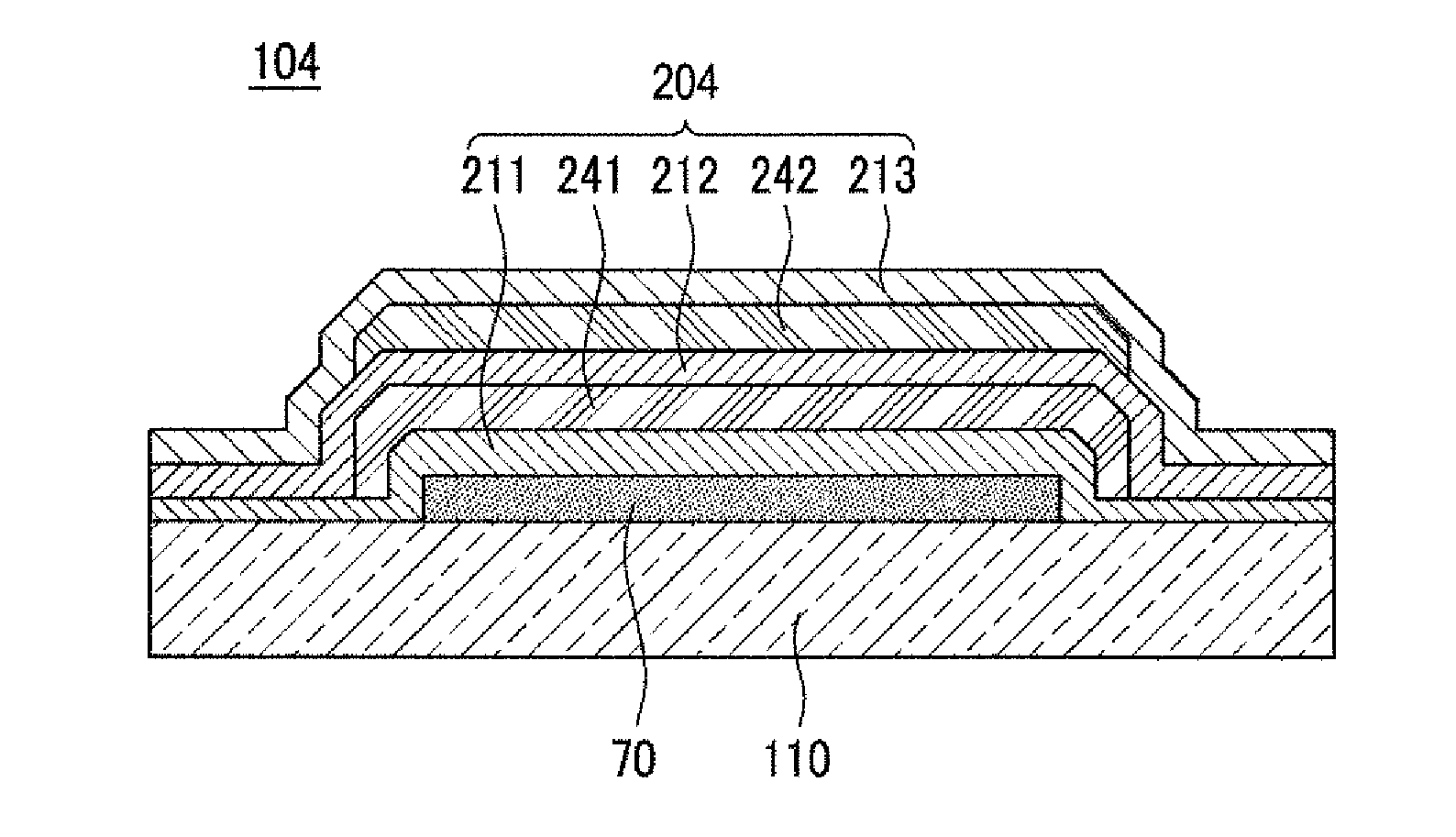
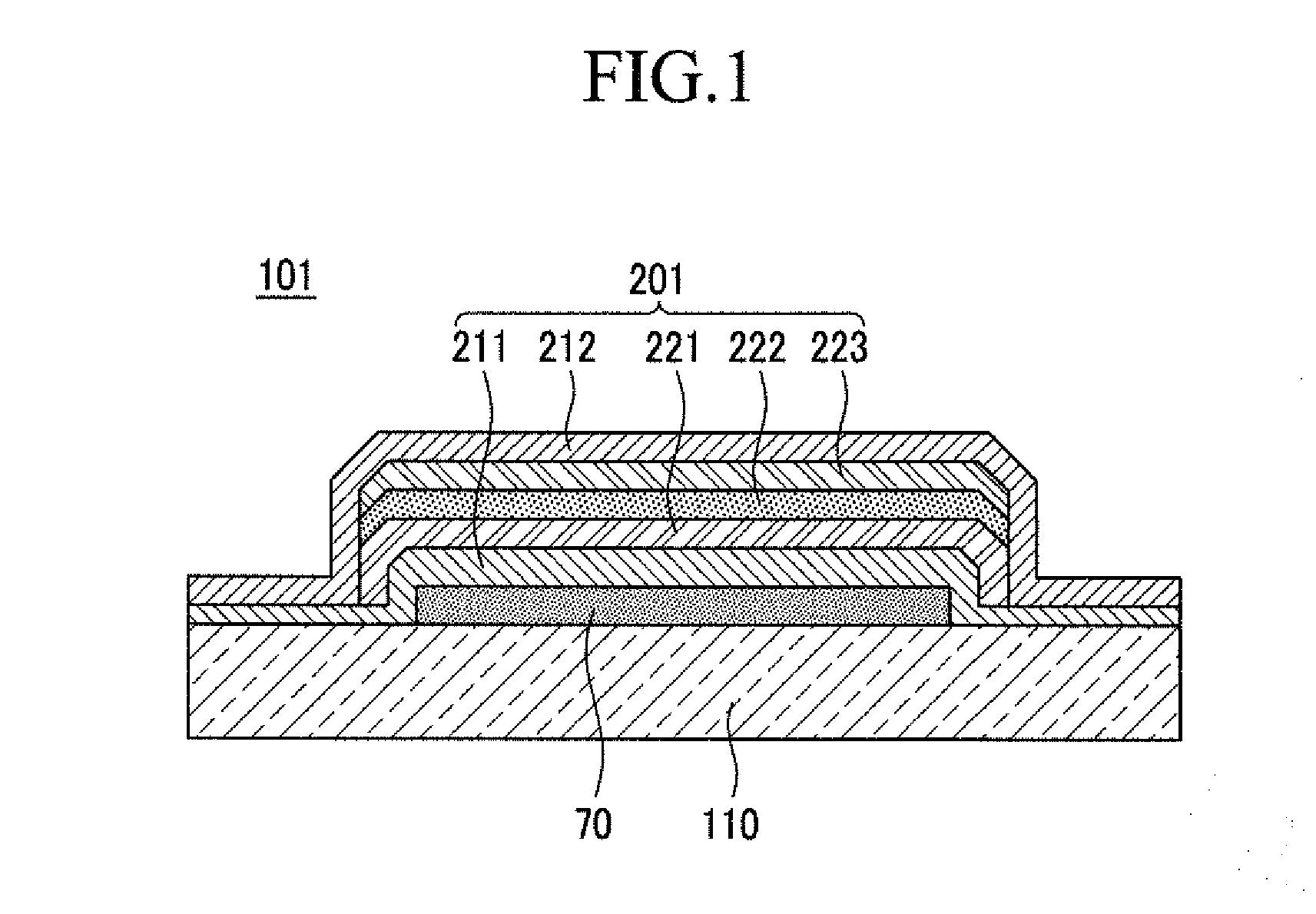
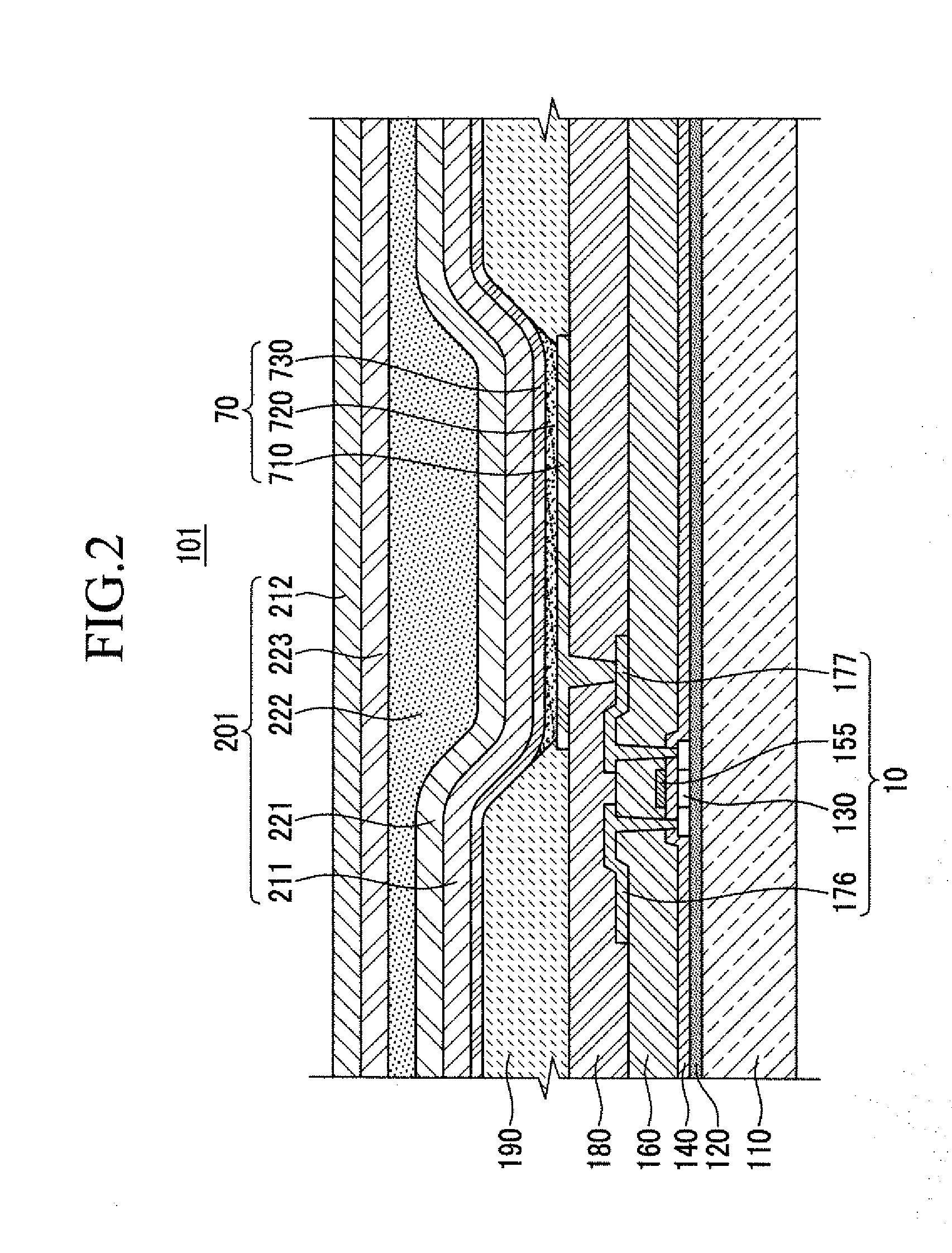
[0042]The present invention will be described more fully hereinafter with reference to the accompanying drawings, in which exemplary embodiments of the invention are shown.

[0043]As those skilled in the art will realize, the described embodiments may be modified in various different ways, all without departing from the spirit or scope of the present invention.

[0044]In various exemplary embodiments, the same reference numerals are used for elements having the same configuration, and will be representatively described in a first exemplary embodiment whereas, in other exemplary embodiments, only elements different from those of the first exemplary embodiment will be described.

[0045]The drawings are schematic and not proportionally scaled down. Relative scales and ratios in the drawings are enlarged or reduced for the purpose of accuracy and convenience, and the scales are random and not limited thereto. In addition, like reference numerals designate like structures, elements, or parts t...


PUM


Abstract

An organic light emitting diode (OLED) display includes: a substrate; an organic light emitting diode formed on the substrate; a first inorganic layer formed on the substrate and covering the organic light emitting diode; an intermediate layer formed on the first inorganic layer and covering an area relatively smaller than the first inorganic layer; and a second inorganic layer formed on the first inorganic layer and the intermediate layer, and contacting the first inorganic layer at an edge thereof while covering a relatively larger area than the intermediate layer. A third inorganic layer may be formed on the second inorganic layer so as to contact the second inorganic layer at an edge thereof. At least one of the first, second and third inorganic layers is formed by an atomic layer deposition (ALD) method.

Description

CLAIM OF PRIORITY[0001]This application makes reference to, incorporates the same herein, and claims all benefits accruing under 35 U.S.C. §119 from an application earlier filed in the Korean Intellectual Property Office on the 14th of October 2011 and there duly assigned Serial No. 10-2011-0105429.BACKGROUND OF THE INVENTION[0002]1. Field of the Invention[0003]The present invention relates to an organic light emitting diode (OLED) display and a manufacturing method thereof. More particularly, the present invention relates to an OLED display using thin film encapsulation, and a manufacturing method thereof.[0004]2. Description of the Related Art[0005]Unlike a liquid crystal display, the OLED display has a self-emitting characteristic and does not need a separate light source such that the thickness and weight thereof are decreased. In addition, since the OLED display involves high quality characteristics such as low power consumption, high luminance, and short response time, it is s...

Claims


Application Information

Patent Timeline
Patent Type & Authority Applications(United States)
IPC IPC(8): H01L51/52H01L51/56
CPCH01L27/3246H01L51/5256H10K59/122H10K50/8445H10K50/844H10K2102/00
Inventor KIM, JIN-KWANGSEO, SANG-JOONKIM, SEUNG-HUN
Owner SAMSUNG DISPLAY CO LTD
Why Eureka
Try Eureka