Thin-film capacitor

a thin film capacitor and capacitor technology, applied in the direction of capacitor details, semiconductor devices, fixed capacitors, etc., can solve the problems of difficult to achieve reliability compatible with practical use and difficult to obtain strong coupling, and achieve excellent i-v characteristics and improve reliability.

Inactive Publication Date: 2013-04-18
TAIYO YUDEN KK
View PDF8 Cites 12 Cited by
  • Summary
  • Abstract
  • Description
  • Claims
  • Application Information

AI Technical Summary

Benefits of technology

[0009]In an MIM-structured thin-film capacitor according to the present invention in which a lower electrode, a dielectric layer, and an upper electrode are laminated in order on a substrate, at least the upper electrode of the upper and lower electrodes is

Problems solved by technology

In addition, since the coupling of a Pt/BST interface is considered to be based on an image force, it is di

Method used


Image

  • Thin-film capacitor
  • Thin-film capacitor
  • Thin-film capacitor

Examples


embodiment 1

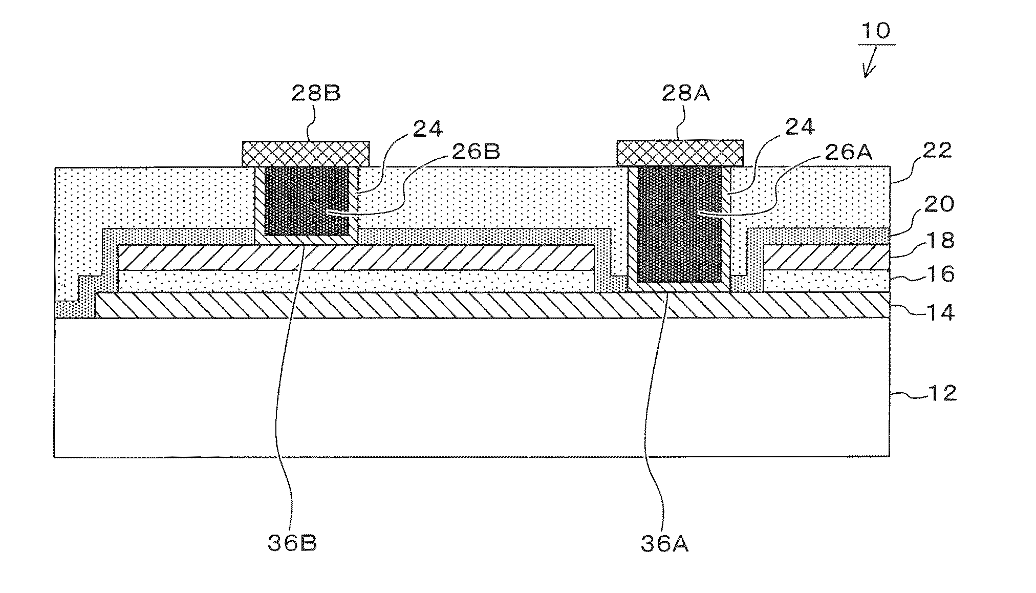
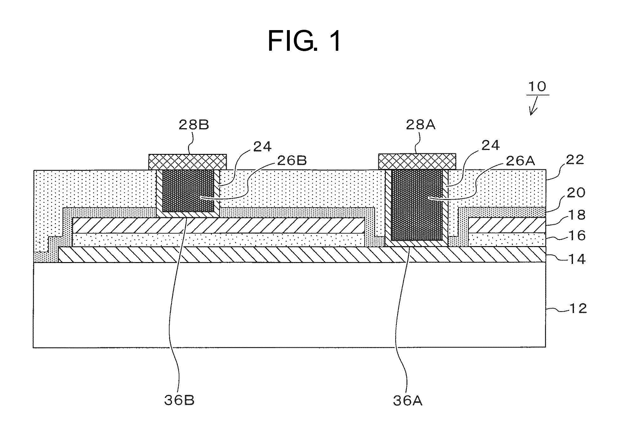
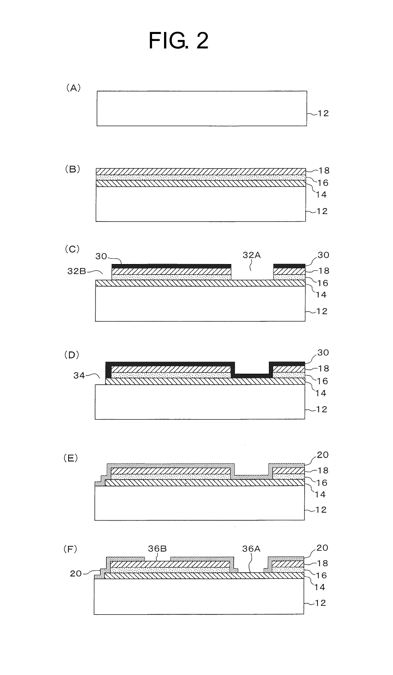
[0018]First, Embodiment 1 of the present invention will be described while referring to FIGS. 1 to 6. In general, a metal large in work function is used as an electrode in an MIM-structured thin-film capacitor. Pt is a metal largest in work function but predisposed to accumulate hydrogen which degrades the characteristics of the MIM capacitor, as described above. Accordingly, forming a thin-film capacitor without using Pt is considered to lead to an essential solution. In order to use a metal small in work function as an electrode, the apparent Schottky barrier of the metal with respect to a dielectric material needs to be heightened. Hence, in the present invention, at least an upper electrode of upper and lower electrodes in contact with a dielectric layer is formed of a laminated electrode in which a nitride and a metal are laminated, thereby controlling the band structure of the dielectric material.

[0019]First, the structure of a thin-film capacitor of the present embodiment wil...


PUM


Abstract

A thin-film capacitor 10 has an MIM structure in which a lower electrode 14, a dielectric layer 16, and an upper electrode 18 are formed in order on a substrate 12. Of the upper and lower electrodes 18 and 14, at least the upper electrode 18 is formed of a laminated electrode in which a nitride and a metal are laminated. The nitride preferably contains a high-melting point metal, such as Ta or Ti. In addition, the metal laminated along with the nitride is preferably the same as the metal contained in the nitride. Yet additionally, the nitride may contain Si. Thus, by using the laminated electrode containing the nitride in at least the upper electrode 18, identical I-V characteristics can be obtained and reliability is improved without the need for an annealing treatment for characteristic recovery necessary when a Pt electrode is used. Still additionally, adhesion between the dielectric layer 16 and the upper electrode 18 is improved, and therefore, delamination does not occur.

Description

TECHNICAL FIELD[0001]The present invention relates to an MIM-structured thin-film capacitor in which a lower electrode, a dielectric layer, and an upper electrode are formed in order on a substrate. More specifically, the present invention relates to the maintenance of I-V characteristics and reliability when an electrode alternative to a Pt electrode is used.BACKGROUND ART[0002]A thin-film capacitor using BaSrTiO3 (hereinafter written as BST or BSTO) or the like as a dielectric layer holds promise for use in decoupling applications in SiP (System In Package) embedded components, taking advantage of the nature of low-profile. FIG. 7 illustrates a conventional MIM-structured thin-film capacitor. A thin-film capacitor 100 illustrated in the FIG. 7 has a structure in which a lower electrode 104, a dielectric layer 106, and an upper electrode 108 are laminated in order on a substrate 102.[0003]In the case where a lower electrode 104 and an upper electrode 108 made of Pt and a dielectric...

Claims


Application Information

Patent Timeline
IPC IPC(8): H01G4/008
CPCH01L27/016H01L28/75H01G4/008H01L28/65H01L28/55
Inventor SASAJIMA, YUICHIHAYAKAWA, ICHIRO
Owner TAIYO YUDEN KK
Why Eureka
Try Eureka