Mosfet and method for manufacturing the same

a technology of mosfet and gate length, which is applied in the field of mosfet, can solve the problems of excessively high threshold voltage of mosfet with a large gate length, short channel effect, and degradation of device performance, and achieve the effect of increasing the threshold voltag

Active Publication Date: 2013-04-25
INST OF MICROELECTRONICS CHINESE ACAD OF SCI
View PDF2 Cites 192 Cited by
  • Summary
  • Abstract
  • Description
  • Claims
  • Application Information

AI Technical Summary

Benefits of technology

[0029]The MOSFET according to the present disclosure comprises the back gate formed in the semiconductor substrate. When a bias voltage is applied to the back gate, the resultant electrical field goes through the buried insulating layer and is applied to the channel region. Thus, the back gate can have an effect of adjusting the threshold voltage, either increasing the threshold voltage or lowering the threshold voltage, depending on the doping type of the back gate.
[0030]In a preferable embodiment of the MOSFET, the anti-doped region is formed in the back gate below the channel region. The anti-doped region has an effect of locally decreasing a doping concentration of the back gate, which avoids excessive adjustment of the threshold voltage, i.e. an excessively high threshold voltage or an excessively low threshold voltage.
[0031]In a preferable embodiment of the MOSFET, the anti-doped region is formed in a MOSFET having a large gate length, but not formed in a MOSFET having a small gate length. Or, the anti-doped region in the MOSFET having a small gate length has a doping concentration higher than that of the anti-doped region in the MOSFET having a large gate length. Therefore, the threshold voltage of the semiconductor device having a small channel length may be adjusted in a way different from the semiconductor device having a large gate length. For example, the adjustment of the back gate in the semiconductor device having a large gate length may be completely suppressed by the anti-doped region. On the other hand, the anti-doped region may not be formed in the semiconductor device having a small gate length, where the back gate still has the effect of suppressing the short channel effects and increasing the threshold voltage.

Problems solved by technology

However, it is well known that short channel effects arise as the sizes of MOSFETs decrease.
Although a high doping concentration in a back gate may be beneficial for the MOSFET with a small gate length for suppressing the short channel effects, it causes an excessively high threshold voltage for the MOSFET with a large gate length.
However, if the threshold voltage of the semiconductor device is raised by increasing a doping concentration in a channel region, the mobility of carriers will drop, which results in degradation of the device performance.

Method used


Image

  • Mosfet and method for manufacturing the same
  • Mosfet and method for manufacturing the same
  • Mosfet and method for manufacturing the same

Examples


Embodiment Construction

[0034]Exemplary embodiments of the present disclosure will be described in more details below with reference to the accompanying drawings. For the sake of clarity, various components in the attached drawings are not drawn to scale.

[0035]Some particular details of the present disclosure will be described below, such as exemplary semiconductor structures, materials, dimensions, process steps and technologies of the semiconductor device, for better understanding of the present disclosure. However, it can be understood by one skilled person in the art that these details are not always essential for but can be varied in a specific implementation of the disclosure. Unless the context clearly indicates otherwise, each part of the semiconductor device can be made of material(s) well known to one skilled person in the art.

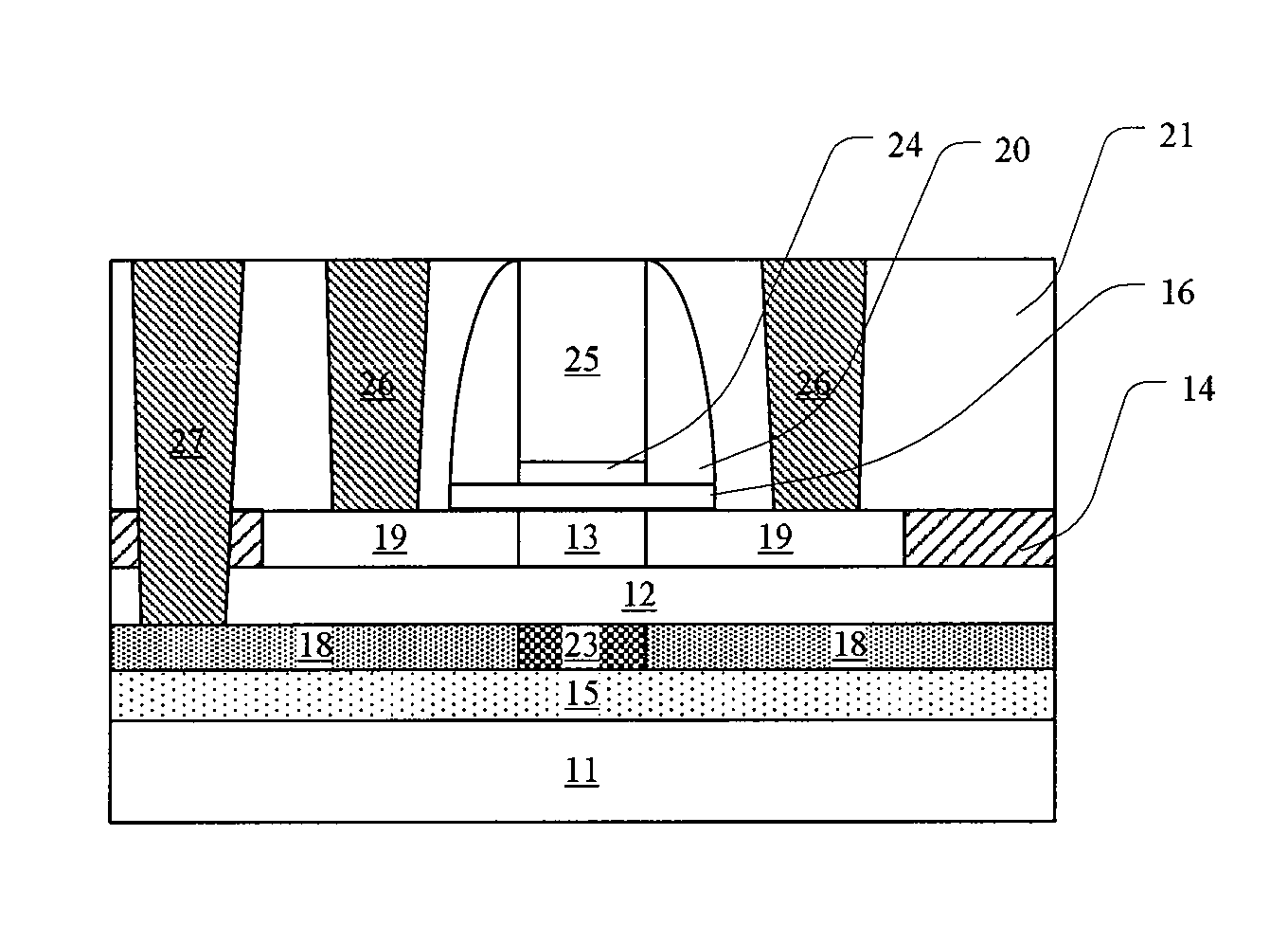
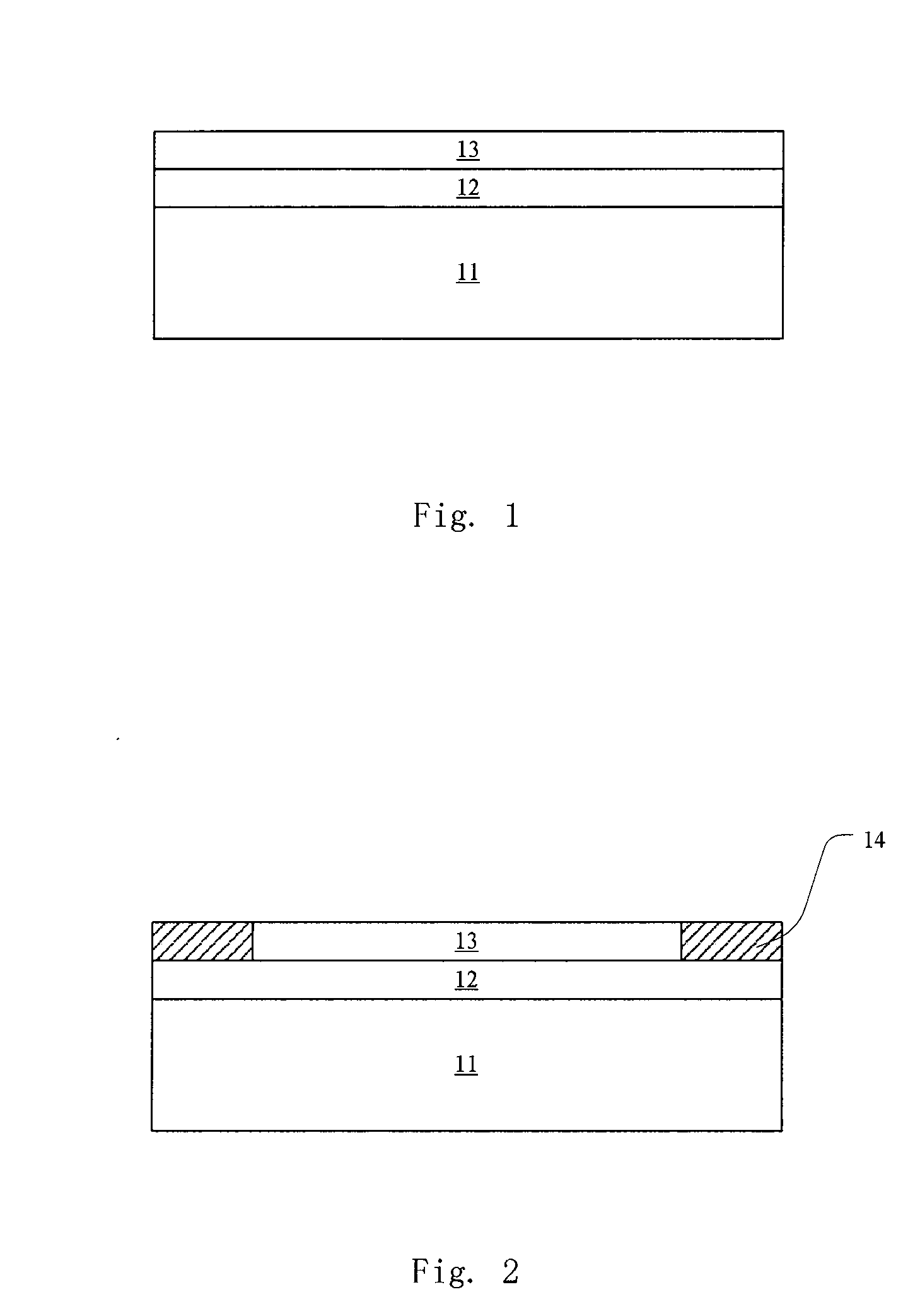
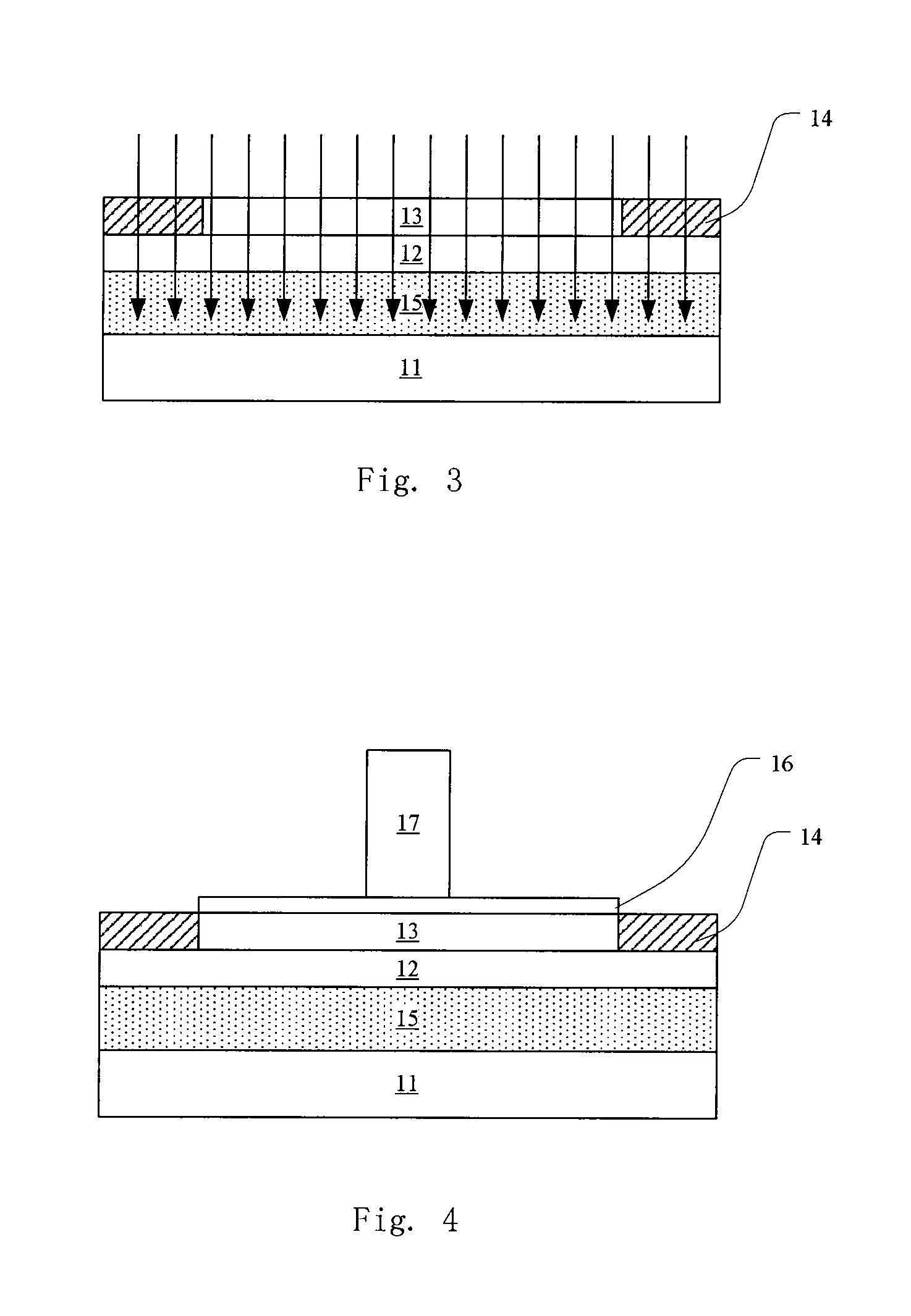
[0036]In the present application, the term “semiconductor structure” means generally the whole semiconductor structure formed at each step of the method for manufacturing t...


PUM

PropertyMeasurementUnit
thicknessaaaaaaaaaa
thicknessaaaaaaaaaa
thicknessaaaaaaaaaa

Abstract

The present disclosure discloses a MOSFET and a method for manufacturing the same, wherein the MOSFET comprises: an SOI wafer which comprises a semiconductor substrate, a buried insulating layer, and a semiconductor layer, the buried insulating layer being on the semiconductor substrate, and the semiconductor layer being on the buried insulating layer; a gate stack on the semiconductor layer; a source region and a drain region, which are in the semiconductor layer and on opposite sides of the gate stack; and a channel region, which is in the semiconductor layer and sandwiched by the source region and the drain region, wherein the MOSFET further comprises a back gate, the back gate being located in the semiconductor substrate and having a first doped region in a lower portion of the back gate and a second doped region in an upper portion of the back gate. The MOSFET can adjust the threshold voltage by changing the doping type and doping concentration of the anti-doped region.

Description

TECHNICAL FIELD[0001]The present disclosure relates to a MOSFET and a method for manufacturing the same, and in particular, to a MOSFET with a back gate and a method for manufacturing the same.BACKGROUND[0002]An important trend in development of semiconductor technology is scaling down of metal-oxide-semiconductor field effect transistors (MOSFETs) for improving integration level and reducing manufacturing cost. However, it is well known that short channel effects arise as the sizes of MOSFETs decrease. As the MOSFETs are scaled down, the gate also has a reduced effective length and actually controls fewer charges in the depletion region when a gate voltage is applied. Consequently, the threshold voltage of the MOSFETs drops with the reduced channel length.[0003]In the MOSFETs, it may be desirable on the one hand that the threshold voltage of the semiconductor device is increased to suppress the short channel effects. On the other hand, it may also be desirable that the threshold vo...

Claims


Application Information

Patent Timeline
Patent Type & Authority Applications(United States)
IPC IPC(8): H01L29/786H01L29/66
CPCH01L29/66742H01L29/78609H01L29/78648
Inventor ZHU, HUILONGXU, MIAOLIANG, QINGQING
Owner INST OF MICROELECTRONICS CHINESE ACAD OF SCI
Why Eureka
Try Eureka