
Semiconductor device and method for fabricating the same

Active Publication Date: 2013-05-02
SK HYNIX INC
View PDF29 Cites 2 Cited by
  • Summary
  • Abstract
  • Description
  • Claims
  • Application Information

AI Technical Summary

Benefits of technology

The invention provides a semiconductor device and a method for making it that includes a bit line formed in pillars. This helps to increase the margin for the bit line process and reduces capacitance between the adjacent bit lines. The method involves forming a first conductive layer over the surface of two pillars, removing the layer from the substrate, and then performing a rapid thermal annealing process. Overall, this helps to improve the performance of the semiconductor device.

Problems solved by technology

In a complicated semiconductor memory apparatus, it is difficult to reduce the whole area by a plurality of transistors included in the semiconductor memory apparatus.

Method used


Image

  • Semiconductor device and method for fabricating the same
  • Semiconductor device and method for fabricating the same
  • Semiconductor device and method for fabricating the same

Examples


Embodiment Construction

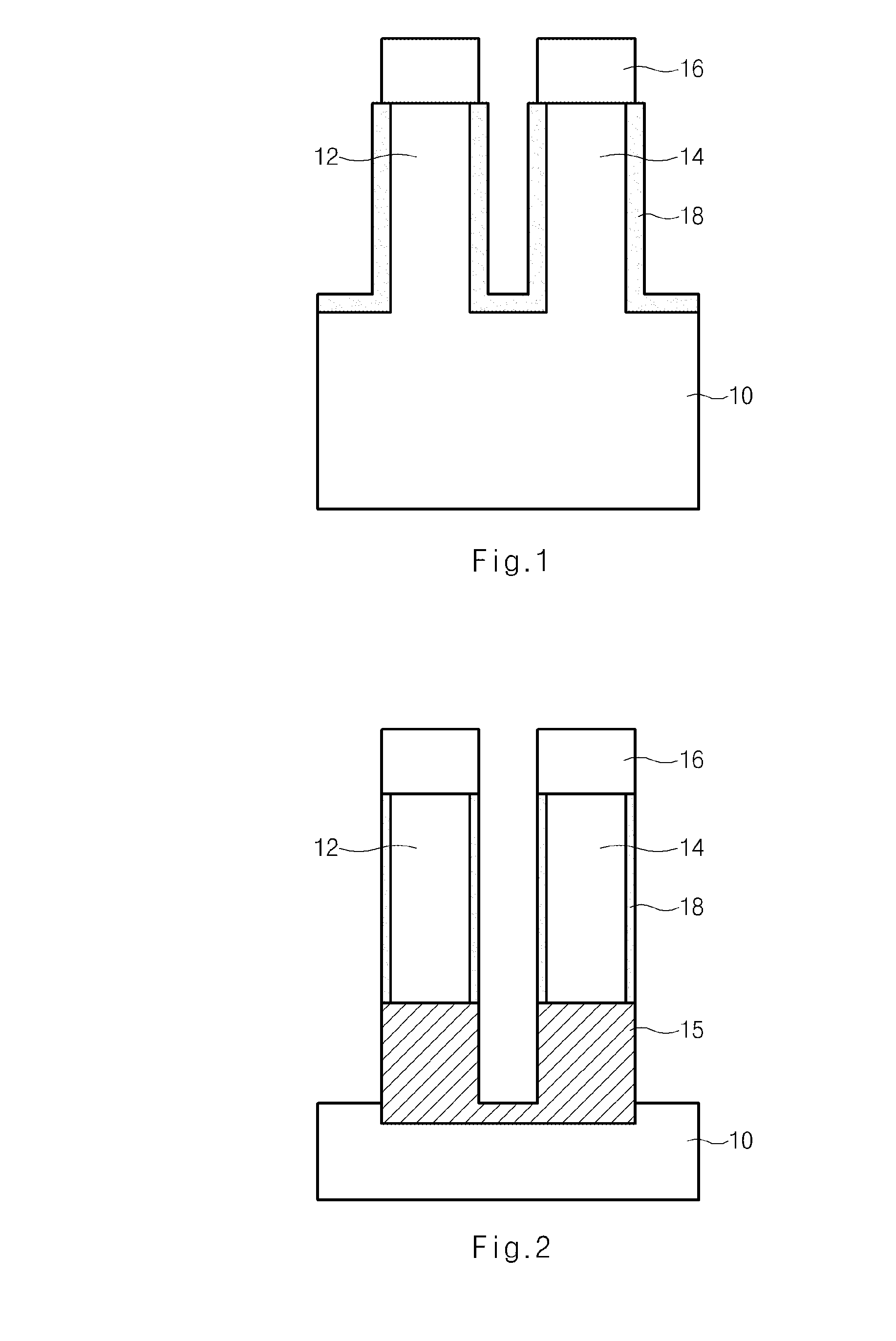
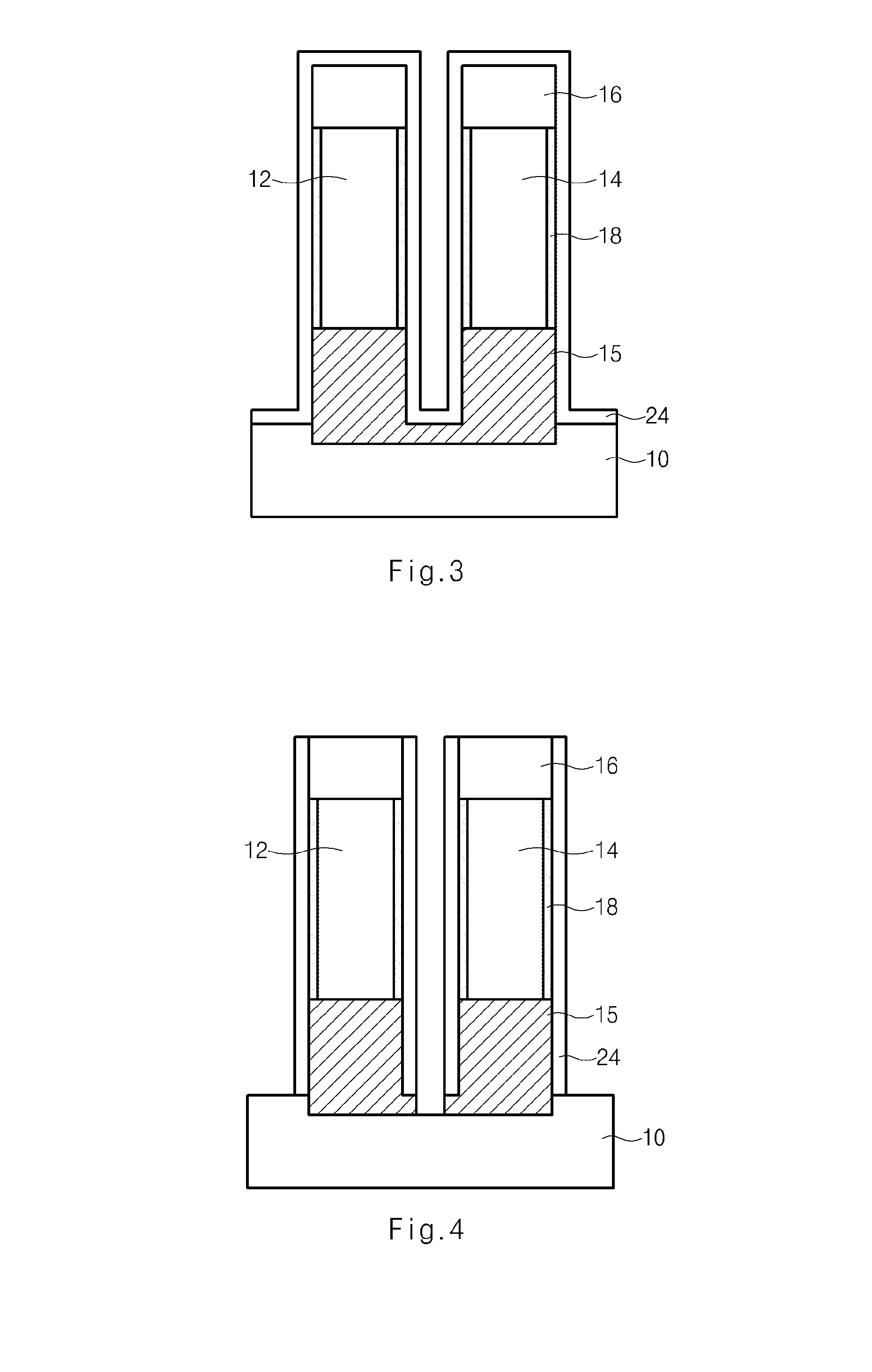
[0049]Exemplary embodiments of the present invention will be described in detail with reference to the attached drawings.

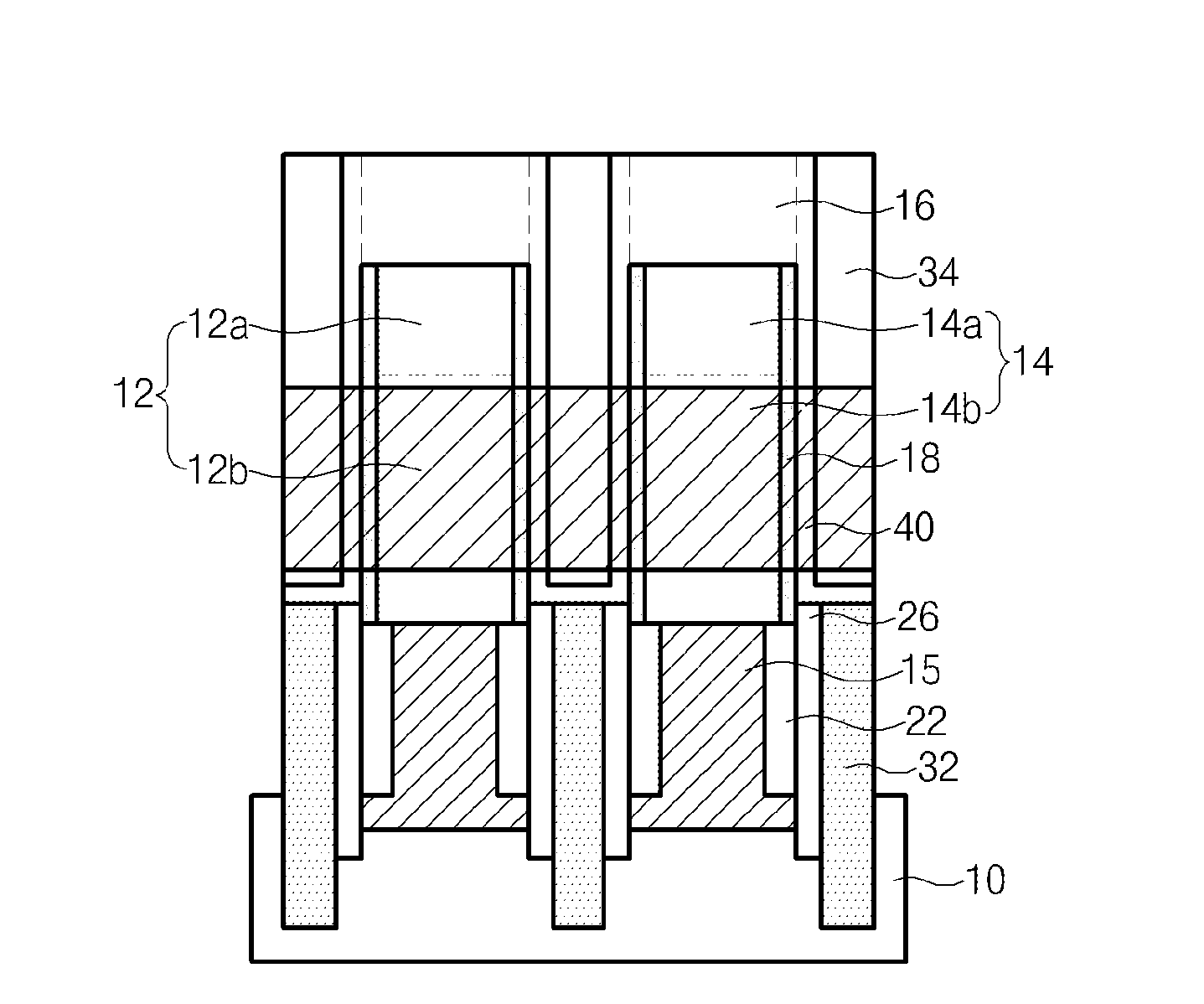
[0050]FIG. 12 is a cross-sectional diagram illustrating a semiconductor device according to an embodiment of the present invention.

[0051]Referring to FIG. 12, pillars 12 and 14 extend in a vertical direction from a semiconductor substrate 10. The two pillars 12 and 14, which are adjacent to each other, are designated as a first pillar 12 and a second pillar 14, respectively. Upper junction regions 12a and 14a are formed in the upper portion of the pillars 12 and 14, vertical channel regions 12b and 14b are formed in the middle portion of the pillars 12 and 14, and a lower junction region 15 is formed in the lower portion of the pillars 12 and 14. Thus, a channel of the transistor is formed along the vertical channel region 12b located between the upper junction region 12a and the lower junction region 15.

[0052]The lower junction region 15 may be formed as an N-typ...


PUM


Abstract

A semiconductor device and a method for fabricating the same are provided to enable a bit line to be formed easily, increase a bit line process margin and reduce capacitance between the adjacent bit lines. The semiconductor device comprises: a first pillar and a second pillar each extended vertically from a semiconductor substrate and including a vertical channel region; a first bit line located in the lower portion of the vertical channel region inside the first pillar and the second pillar; and an interlayer insulating film located between the first pillar and the second pillar that include the first bit line.

Description

CROSS-REFERENCE TO RELATED APPLICATION[0001]The present application claims priority to Korean patent application No. 10-2011-0112418 filed on Oct. 31, 2011, which is incorporated by reference in its entirety.BACKGROUND OF THE INVENTION[0002]1. Technical Field[0003]The inventive concept relates generally to a semiconductor device and a method for fabricating the same, and more particularly to a semiconductor device that comprises a vertical channel transistor and a method for fabricating the same.[0004]2. Related Art[0005]In general, a semiconductor, as a material which belongs in an intermediate range between a conductor and a nonconductor by material classification depending on electric conductivity, has similar properties as a pure nonconductor, but its electric conductivity may be increased by the addition of impurities or by other manipulations. A semiconductor material is used for generating a semiconductor device such as a transistor by adding impurities and connecting device ...

Claims


Application Information

Patent Timeline
IPC IPC(8): H01L27/108
CPCH01L29/41741H01L29/456H01L29/66666H01L27/10885H01L27/10823H01L27/10876H01L29/7827H10B12/34H10B12/053H10B12/482H01L29/66712
Inventor KIM, SEUNG HWAN
Owner SK HYNIX INC
Learn More