Two-dimensional shielded gate transistor device and method of manufacture

Active Publication Date: 2013-05-02
ALPHA & OMEGA SEMICON INC
View PDF2 Cites 21 Cited by
  • Summary
  • Abstract
  • Description
  • Claims
  • Application Information

AI Technical Summary

Benefits of technology

[0045]Embodiments of the present invention allow for independent optimization of the cell pitch and shield electrode pitch when scaling down the cell pitch for shielded gate tran

Problems solved by technology

However, for the low-side switch which operates as a synchronous rectifier, excessive charge during the reverse recovery of the body diode results in increased power dissipa

Method used


Image

  • Two-dimensional shielded gate transistor device and method of manufacture
  • Two-dimensional shielded gate transistor device and method of manufacture
  • Two-dimensional shielded gate transistor device and method of manufacture

Examples


embodiments

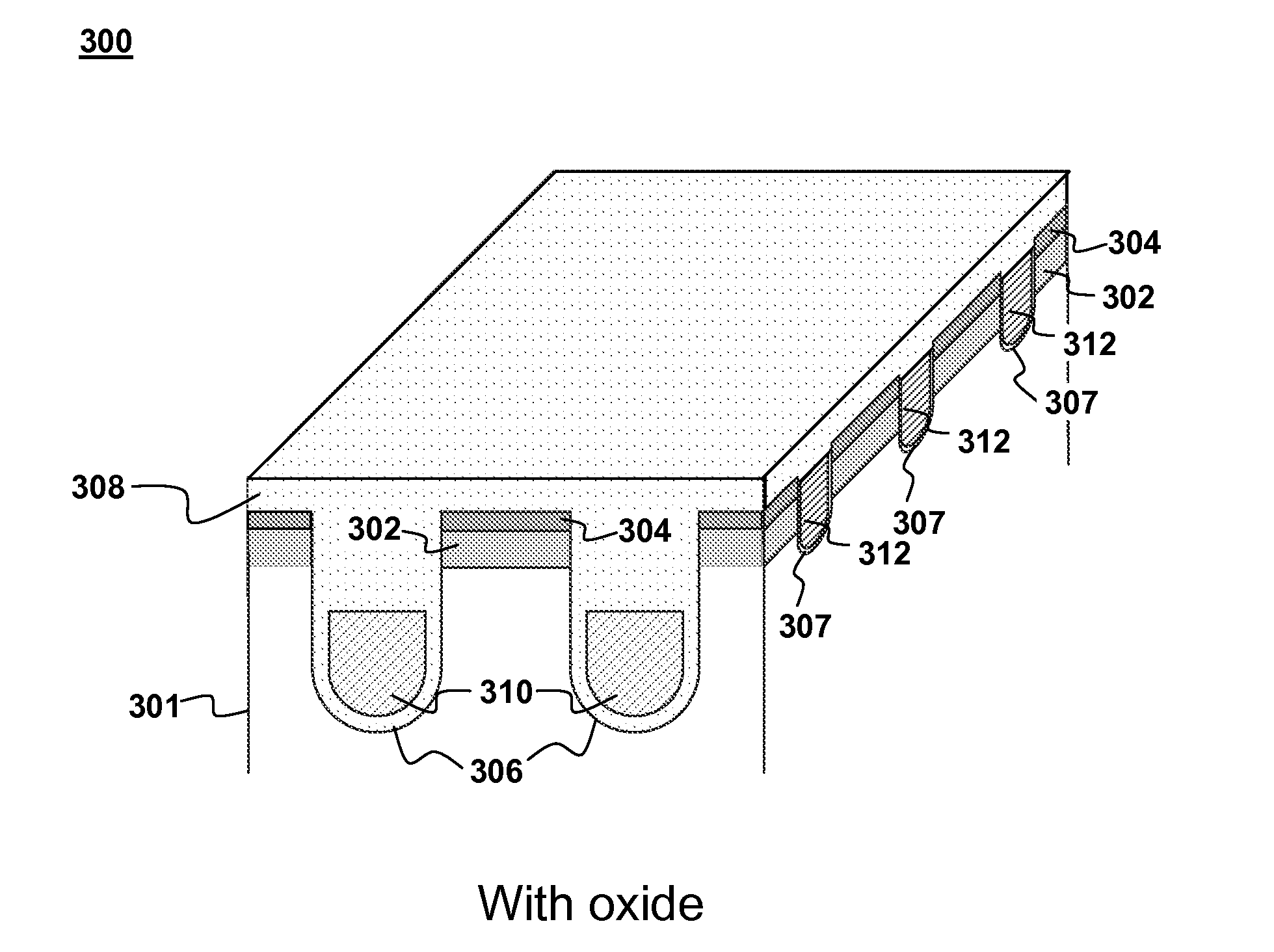
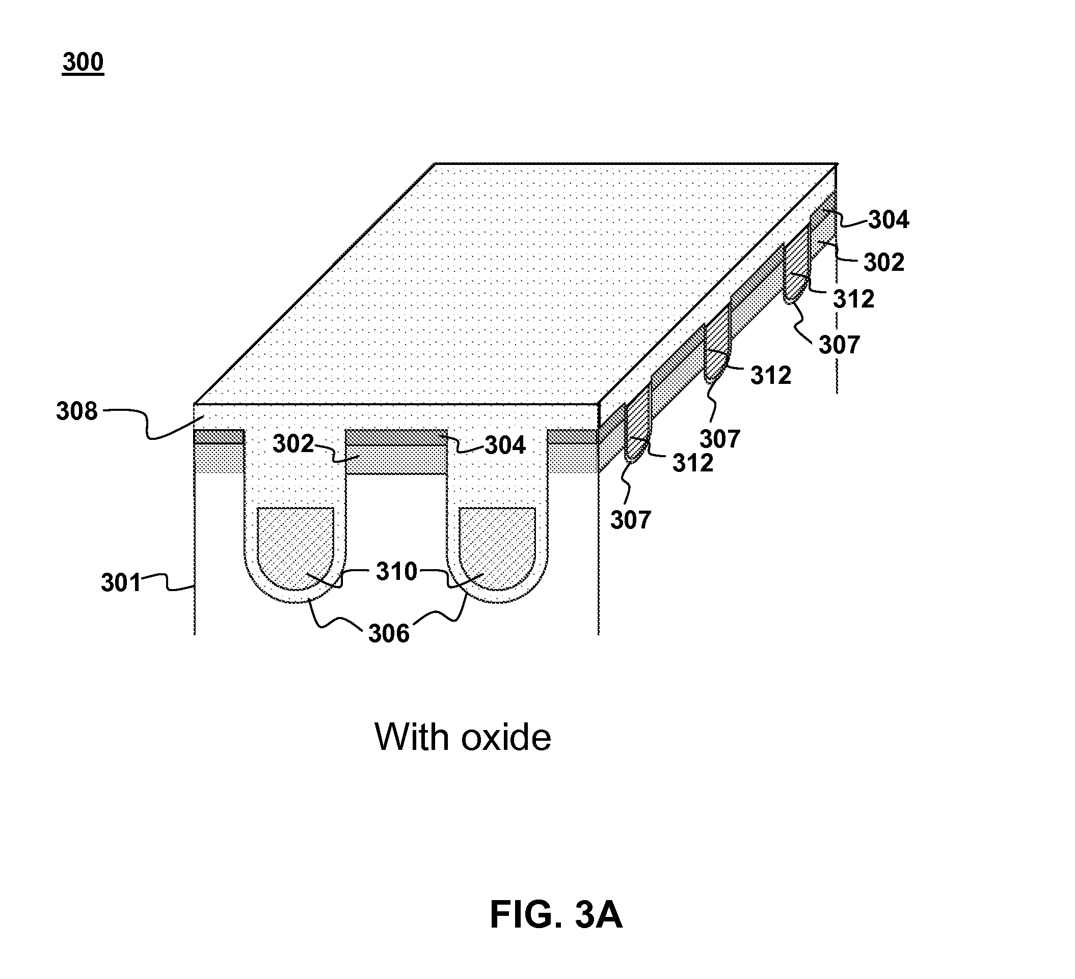
[0033]FIGS. 3A-3G illustrate a portion of a shielded gate transistor device 300 according to an embodiment of the present invention. The device 300 is formed on a semiconductor substrate 301, which may be made of suitably doped silicon. A lower portion of the substrate 301 may be doped to provide a desired first conductivity type (e.g., N-type or P-type). The lower portion of the substrate 301 can act as a drain for the device 300. Similar to the device 100, a body portion 302 and source regions 304 are formed in upper portions of the substrate 301. The body portion 302 is doped with dopants that provide the body portion with a second conductivity type that is opposite to the first conductivity type of the lower portions. The source regions 304 are doped with dopants with the first conductivity type but more heavily doped than the lower portion of substrate 301. By way of example and not by way of limitation, the lower portions of the substrate 301 may be doped with N-type dopant, t...


PUM


Abstract

A shielded gate transistor device may include one or more shield electrodes formed in a semiconductor substrate at a first level and one or more gate electrodes formed in the semiconductor substrate at a second level that is different from the first level. One or more portions of the one or more gate electrodes overlap one or more portions of the one or more shield electrodes. At least a portion of the gate electrodes is oriented non-parallel to the one or more shield electrodes. The shield electrodes are electrically insulated from the semiconductor substrate and the one or more gate electrodes are electrically insulated from the substrate and shield electrodes.

Description

FIELD OF THE INVENTION[0001]This invention relates in general to transistors and more particularly to shielded gate transistor devices and methods of manufacturing such devices.BACKGROUND OF THE INVENTIONS[0002]Shielded gate transistors are preferred for certain applications over conventional transistors, such as conventional trench MOSFETs (metal oxide semiconductor field effect transistors) because they provide several advantageous characteristics. Shielded gate trench transistors (SGTs) exhibit reduced gate-to-drain capacitance Cgd, reduced on-resistance RDSon, and increased breakdown voltage of the transistor. For conventional trench MOSFETs, the placement of many trenches in a channel, while decreasing the on-resistance, also increased the overall gate-to-drain capacitance. The introduction of the shielded gate trench MOSFET structure remedies this issue by shielding the gate from the electric field in the drift region, thereby substantially reducing the gate-to-drain capacitan...

Claims


Application Information

Patent Timeline
IPC IPC(8): H01L29/78
CPCH01L29/407H01L29/4236H01L29/7813H01L29/66734H01L29/4238
Inventor LUI, SIKBHALLA, ANUPNG, DANIEL
Owner ALPHA & OMEGA SEMICON INC
Why Eureka
Try Eureka