Semiconductor device having extra capacitor structure and manufacturing method thereof

Active Publication Date: 2012-03-01
SINOPOWER SEMICON
View PDF3 Cites 19 Cited by
  • Summary
  • Abstract
  • Description
  • Claims
  • Application Information

AI Technical Summary

Benefits of technology

[0012]In accordance with the present invention, the transistor device and the extra capacitor structure are fabricated in the same semiconductor device and electrically connected to the same drain metal layer and the source metal layer. Thus, an output capacitance of the semiconductor device can be raised. Accordingly, the voltage spike can be reduced, and the power loss can be lowered when the semiconductor device is switched off. Moreover, the

Problems solved by technology

However, the converter further includes an inductor device, so that the output capacitor and the inductor device constitute an LC resonant circuit when the trench NMOSFET device is switched off, and a voltage spike is accordingly generated.
Accordingly,

Method used


Image

  • Semiconductor device having extra capacitor structure and manufacturing method thereof
  • Semiconductor device having extra capacitor structure and manufacturing method thereof
  • Semiconductor device having extra capacitor structure and manufacturing method thereof

Examples


Embodiment Construction

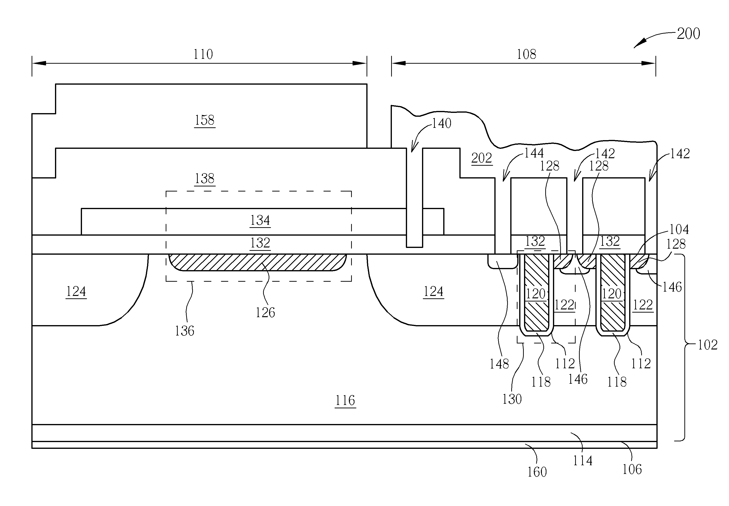
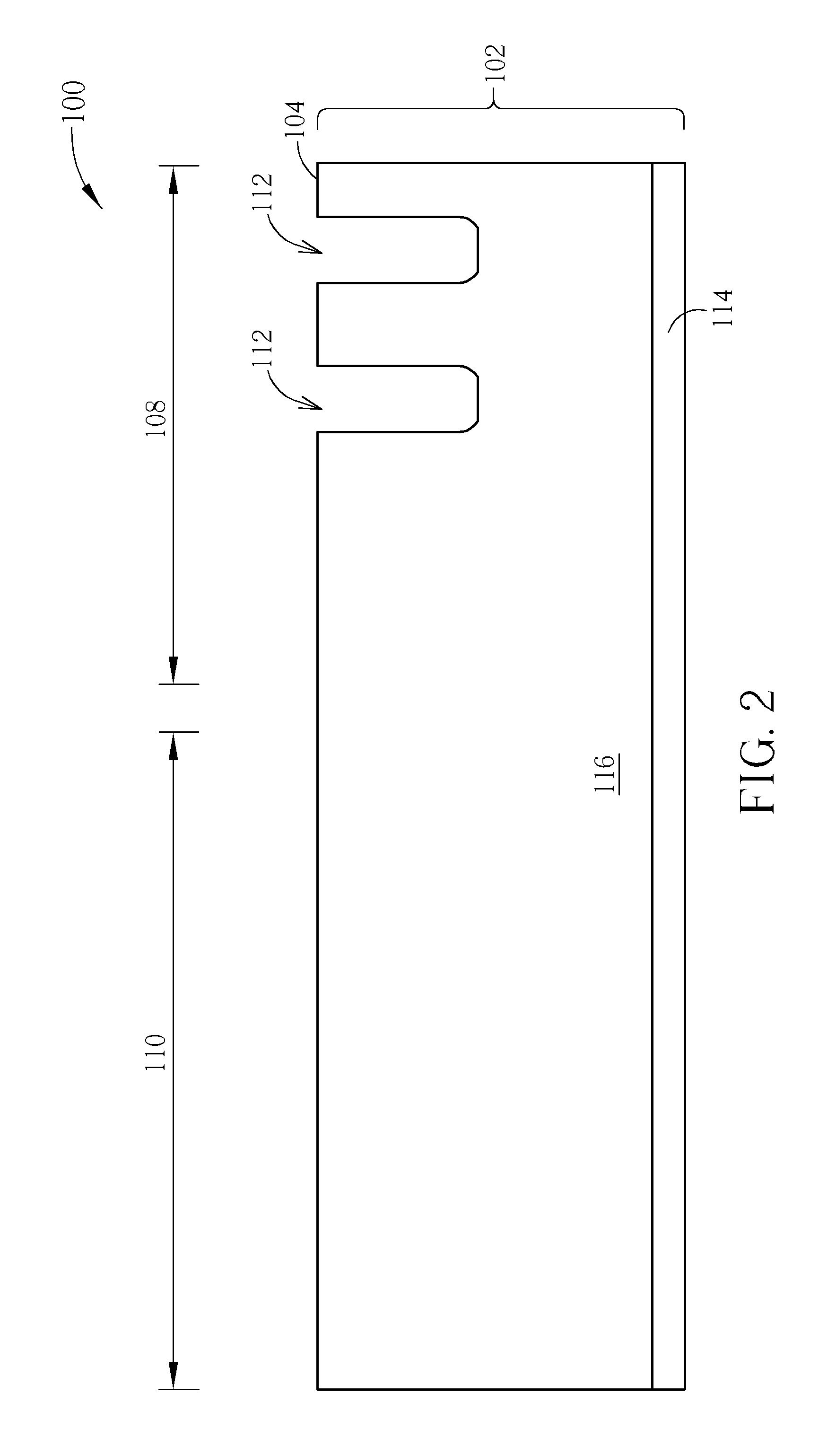
[0018]Please refer to FIG. 2 through FIG. 7, which schematically illustrate a manufacturing method of a semiconductor device having an extra capacitor structure according to a first embodiment of the present invention. As shown in FIG. 2, a semiconductor substrate 102 is provided at first, and the semiconductor substrate 102 has an upper surface 104 and a lower surface 106. Additionally, the semiconductor substrate 102 has a first pad region 108 and a second pad region 110, and the upper surface 104 of the semiconductor substrate 104 in the first pad region 108 has at least one trench 112. In this embodiment, the first pad region 108 is defined as a region for disposing a source pad, and the second pad region 110 is defined as a region for disposing a gate pad, but not limited thereto. The semiconductor substrate 102 has a first conductive type, and the first conductive type is N type for example, but not limited thereto. Specifically, the step of providing the N-semiconductor subst...


PUM


Abstract

A semiconductor device includes a semiconductor substrate having a conductive type, a source metal layer, a gate metal layer, at least one transistor device, a heavily doped region having the conductive type, a capacitor dielectric layer, a conductive layer. The source metal layer and the gate metal layer are disposed on the semiconductor substrate. The transistor device is disposed in the semiconductor substrate under the source metal layer. The heavily doped region, the capacitor dielectric layer and the conductive layer constitute a capacitor structure, disposed under the gate metal layer, and the capacitor structure is electrically connected between a source and a drain of the transistor device.

Description

BACKGROUND OF THE INVENTION[0001]1. Field of the Invention[0002]The present invention relates to a semiconductor device and a manufacturing method thereof, and more particularly, to a semiconductor device having an extra capacitor structure and a manufacturing method thereof.[0003]2. Description of the Prior Art[0004]Power semiconductor devices are mainly applied to power management devices, such as switching power supplies, power management integrated circuits for computers or computer accessories, backlight power supplies and motor control devices, etc., and can be sorted as metal-oxide-semiconductor thin film transistor (MOSFET) devices and insulated gate bipolar transistor (IGBT) devices, etc. In general, the power semiconductor devices are designed with trenches to lower power consumptions.[0005]However, electronic products are developed toward lighter, thinner, shorter, and smaller designs, so that sizes and gaps of the trench MOSFET devices are continuously scaled down to hav...

Claims


Application Information

Patent Timeline
IPC IPC(8): H01L29/94H01L21/336
CPCH01L28/60H01L29/41766H01L29/66727H01L29/7813H01L29/7803H01L29/7811H01L29/66734
Inventor LIN, WEI-CHIEH
Owner SINOPOWER SEMICON
Why Eureka
Try Eureka