

Micromachined on-wafer probes and related method
- Summary
- Abstract
- Description
- Claims
- Application Information
AI Technical Summary
Benefits of technology
Problems solved by technology
Method used
Image

Examples
example 1
[0170 includes a device for probing a structure on a surface of an object substrate, said device comprising:[0171]a microfabricated compliant chip, wherein said microfabricated compliant chip comprises integrated electrical interconnects.
[0172]Example 2 may optionally include the device of example 1, wherein said microfabricated compliant chip is monolithic.
[0173]Example 3 may optionally include the device of example 1, wherein the structure on the object substrate comprises at least one of the following: microelectronic device; Microelectromechanical (MEM) device, material, or non-electronic device.
[0174]Example 4 may optionally include the device of example 1, wherein the material comprises a biological material, graphene, an atomic scale lattice structure, or an atomic scale lattice structure.
example 5
[0175 may optionally include the device of example 1, wherein the surface on the object substrate comprises at least one of the following: an integrated circuit.
[0176]Example 6 may optionally include the device of example 1, wherein the surface on the object substrate comprises at least one of the following: sample of material with appropriate contacts or some other geometric feature that has been fabricated on the substrate surface.
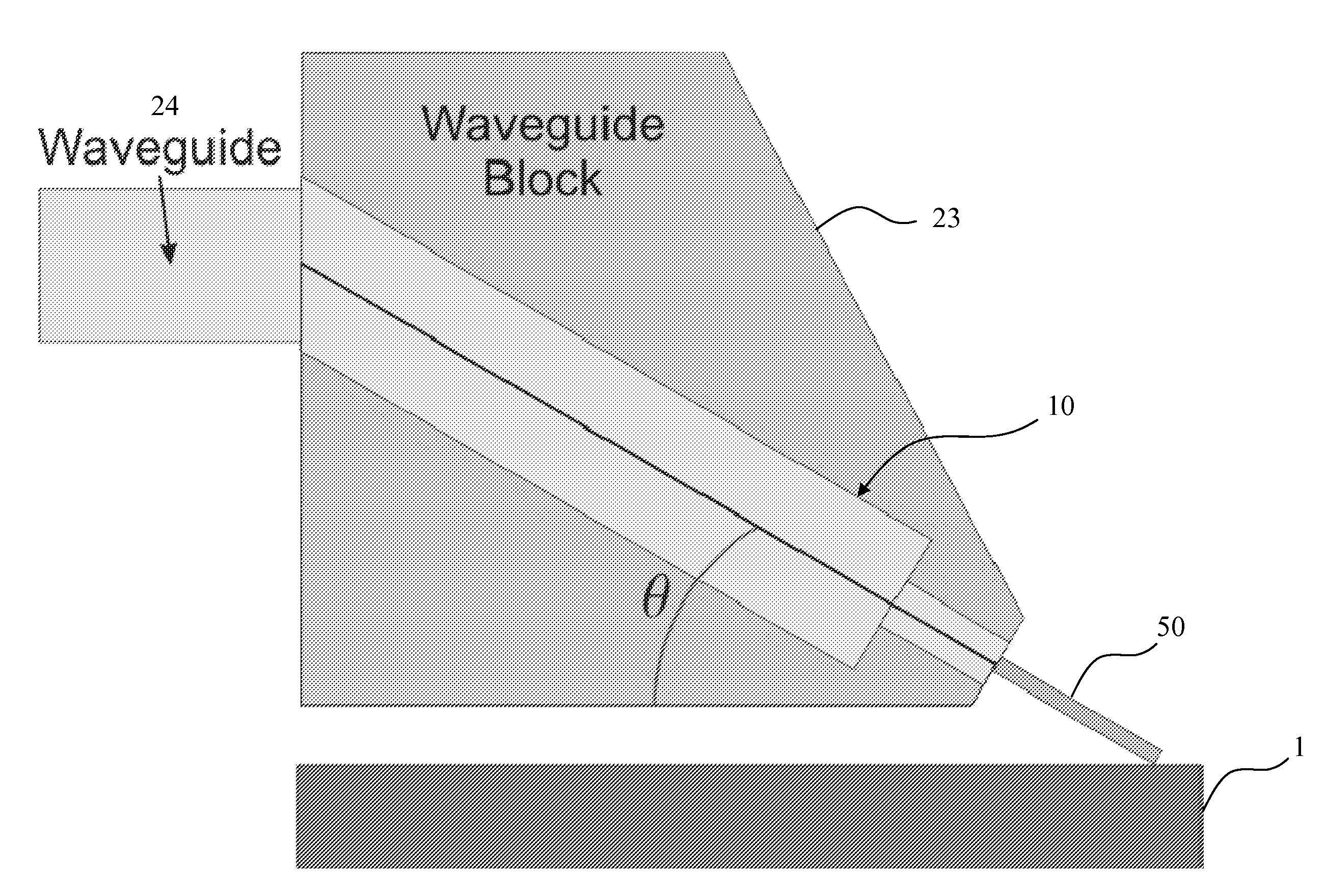
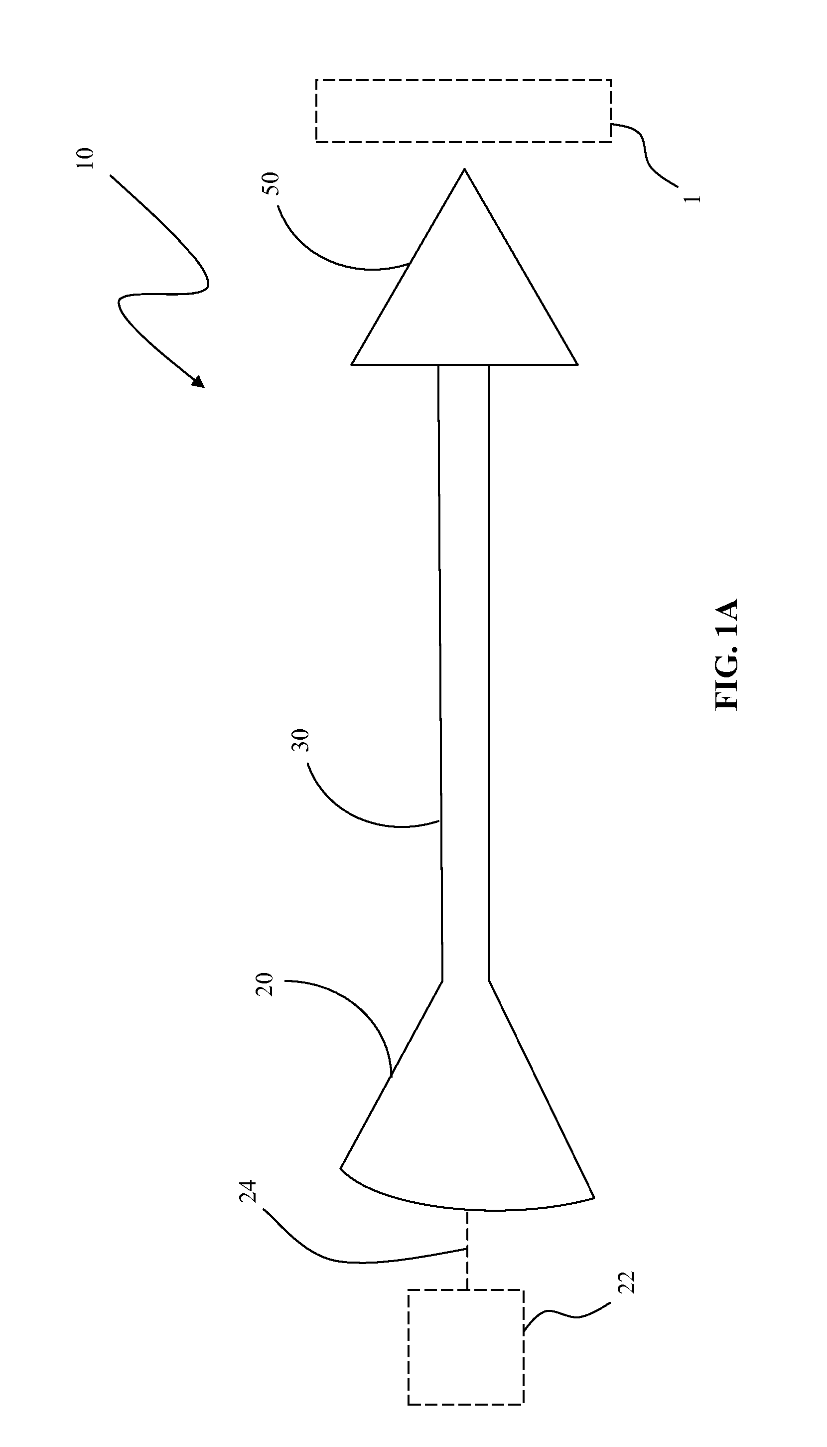
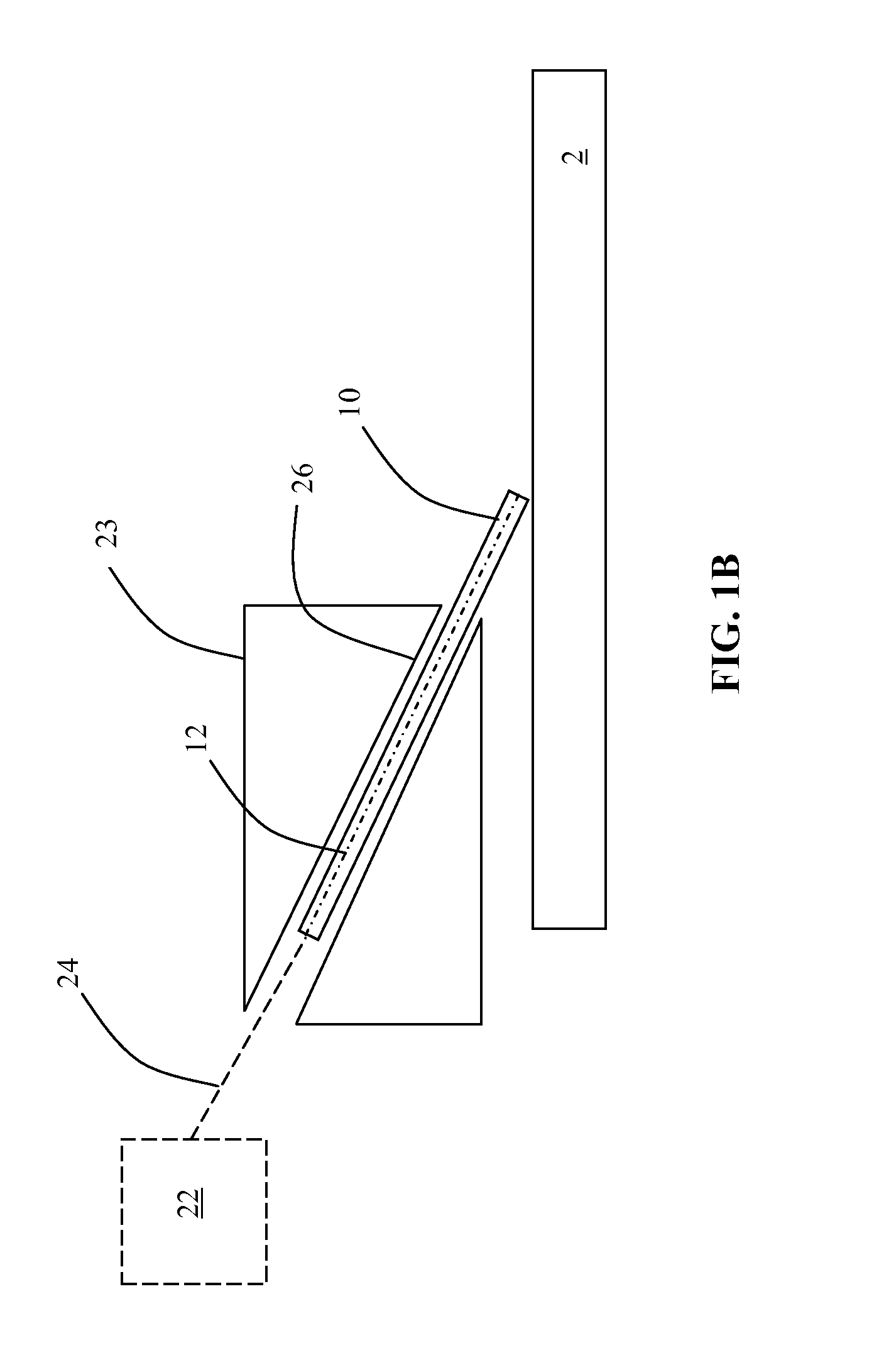
[0177]Example 7 may optionally include the device of example 1, wherein said integrated electrical interconnects of said microfabricated compliant chip comprise:[0178]at least one compliant beam;[0179]at least one transmission circuit; and[0180]a waveguide transition element, wherein said at least one transmission circuit suitable to electrically interconnect said at least one compliant beam with said waive guide transition element.
[0181]Example 8 may optionally include the device of example 7, wherein said compliant beam is monolithic.
[0182]Example 9 ma...
example 13
[0186 may optionally include the device of example 11, wherein said securement provided by compressive forces.
[0187]Example 14 may optionally include the device of example 13, wherein said compressive forces being adjustable.
[0188]Example 15 may optionally include the device of example 11 or 12, wherein said housing comprises an aperture configured to receive said microfabricated compliant chip.
[0189]Example 16 may optionally include the device of example 15, wherein said housing aperture comprises at least one of the following: slot, groove, recess, channel, tunnel, indentation, passage, split, or port.
[0190]Example 17 may optionally include the device of example 11 or 12, wherein said housing is configured to be re-usable when said microfabricated compliant chip is detached and replaced with another microfabricated compliant chip.
[0191]Example 18 may optionally include the device of example 7, wherein said integrated electrical interconnects of said microfabricated compliant chip ...
PUM
 Abstract
Description
Claims
Application Information