

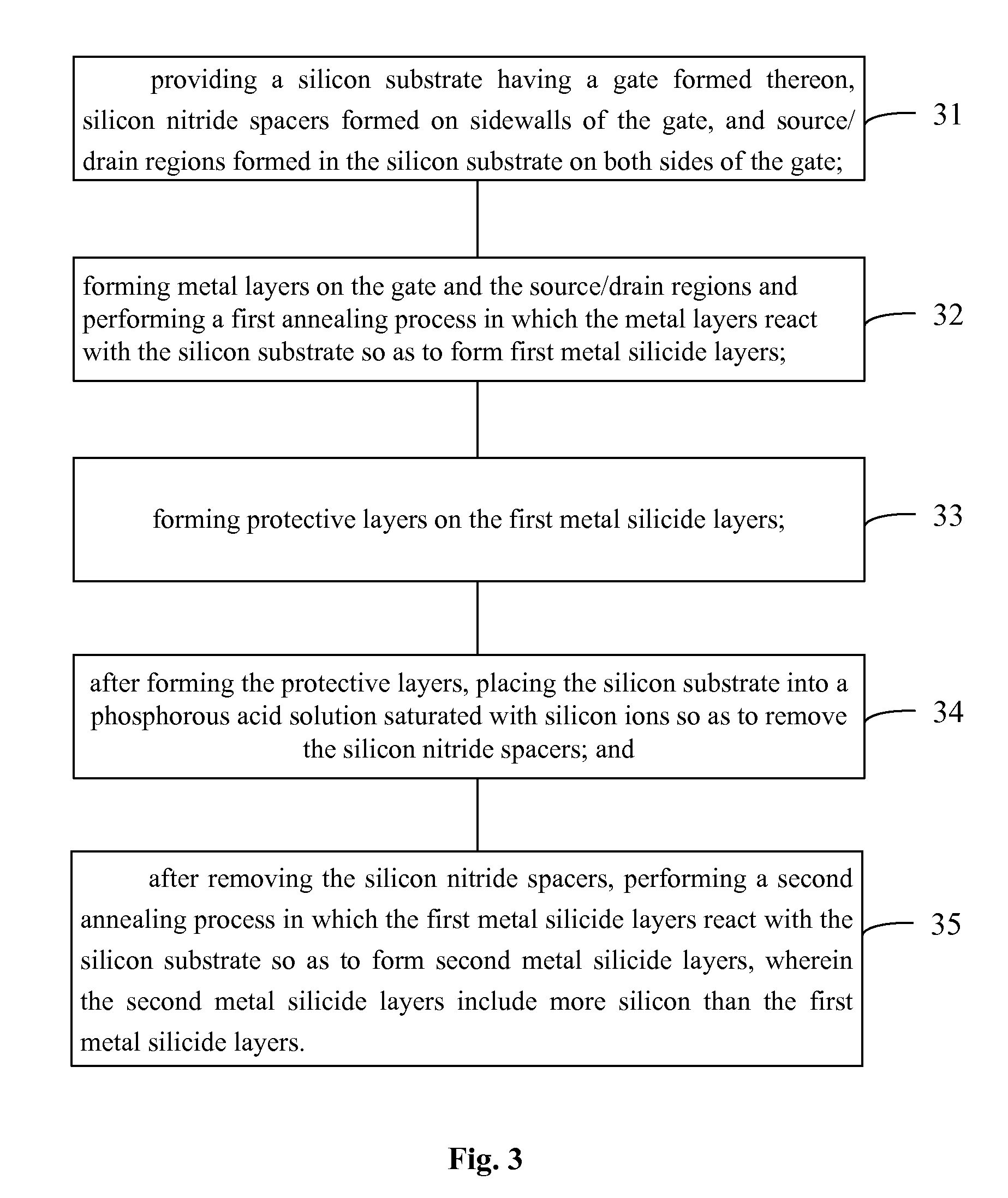
Methods for removing silicon nitride spacer, forming transistor and forming semiconductor devices
a silicon nitride and spacer technology, applied in the field of semiconductor manufacturing, can solve the problems of reducing the contact resistance of the plug, adding process time, and reducing production efficiency, so as to reduce the loss of the first metal silicide layer, reduce process time and production cost, and less silicon
- Summary
- Abstract
- Description
- Claims
- Application Information
AI Technical Summary
Benefits of technology
Problems solved by technology
Method used
Image

Examples
Embodiment Construction
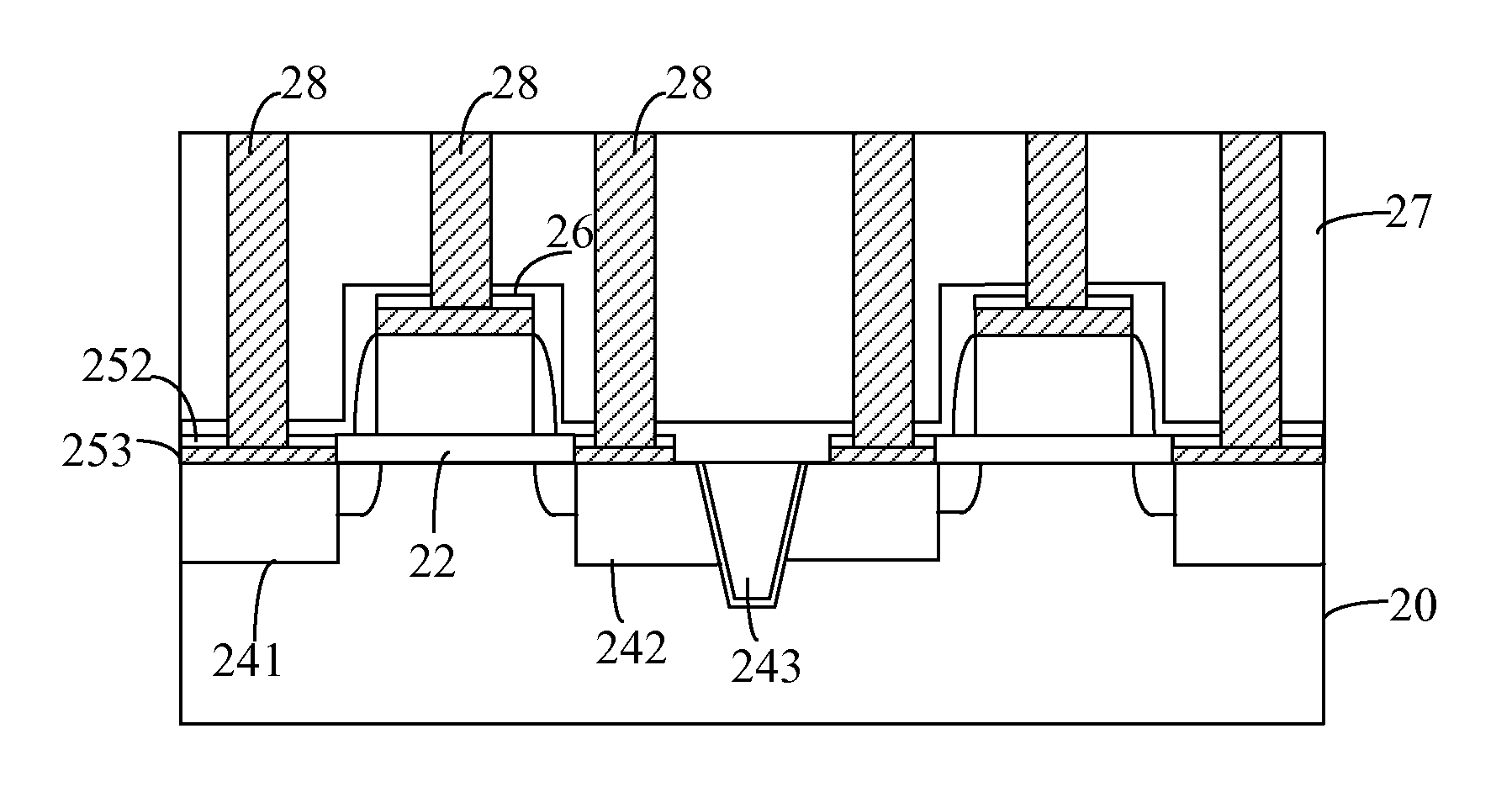
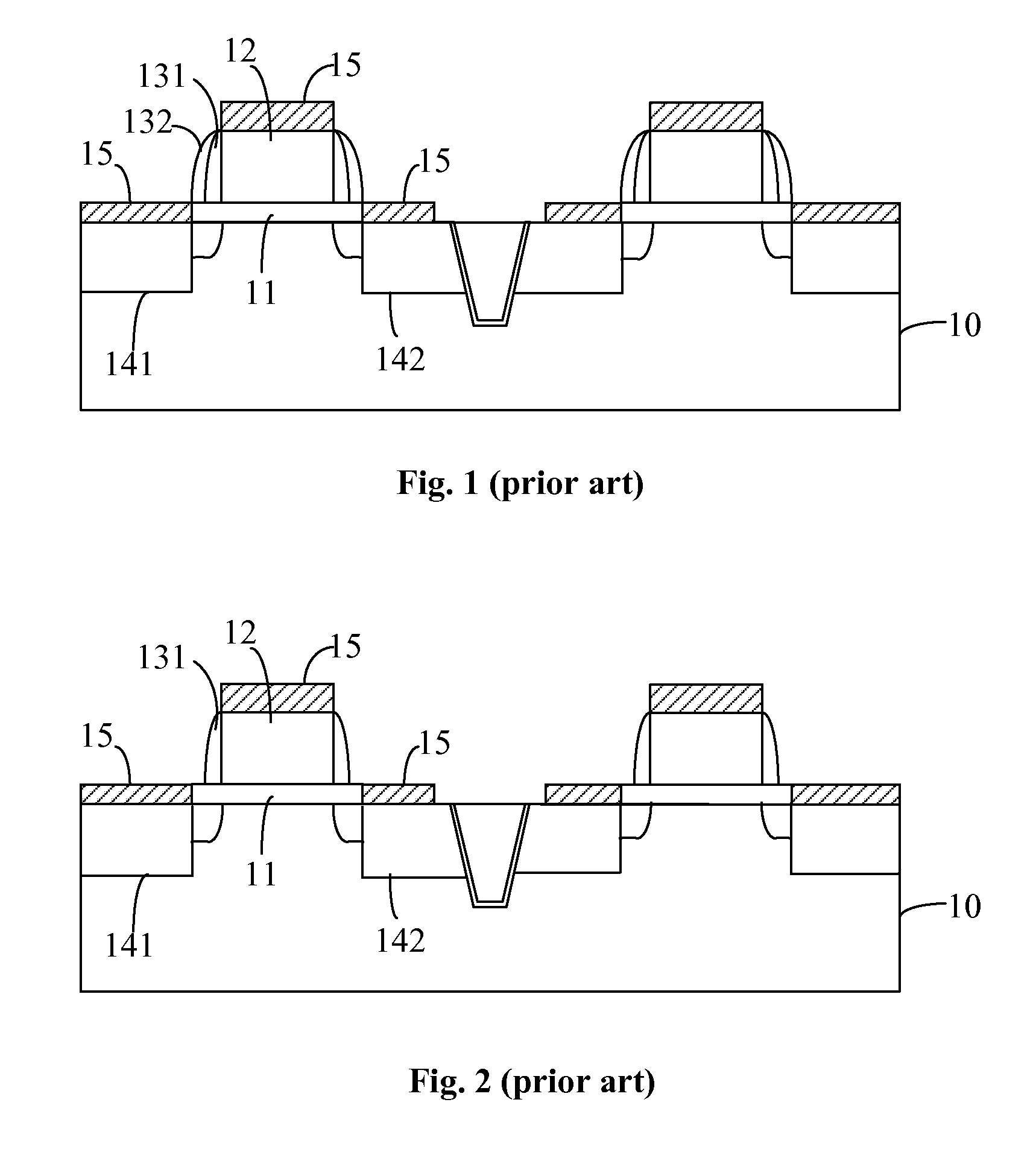
[0035]The inventor of the present invention discovered that, when 50 wafers having silicon nitride surfaces are placed into a phosphorous acid solution at a temperature of about 160° C. as described in the prior art, there is a need to wait 48 hours for the temperature of the phosphorous acid solution to drop from about 160° C. to about 140° C. because the number of wafers is not sufficiently large to quickly make the phosphorous acid solution saturated. In order to save time and avoid a long wait time for the temperature of the phosphorous acid solution to drop, more wafers having silicon nitride surfaces need to be placed into the phosphorous acid solution, the number of wafers should be sufficiently large to quickly make the phosphorous acid solution saturated at a temperature of about 160° C. However, when a substrate having silicon nitride spacers is directly placed into the saturated phosphorous acid solution at a temperature of about 160° C., the loss of metal silicide is lar...
PUM
| Property | Measurement | Unit |
|---|---|---|
| temperature | aaaaa | aaaaa |
| temperature | aaaaa | aaaaa |
| volume | aaaaa | aaaaa |
Abstract
Description
Claims
Application Information