Electroplating Solutions and Methods For Deposition of Group IIIA-VIA Films

a technology of group iiia-via and electroplating solution, which is applied in the direction of sustainable manufacturing/processing, climate sustainability, and final product manufacturing, etc., can solve the problems of high cost of capital equipment, high cost of electricity generated by silicon-based solar cells, and relatively slow production ra

Inactive Publication Date: 2013-05-09
SOLOPOWER
View PDF0 Cites 25 Cited by
  • Summary
  • Abstract
  • Description
  • Claims
  • Application Information

AI Technical Summary

Benefits of technology

[0008]One technique employed for growing Cu(In,Ga)(S,Se)2 type compound thin films for solar cell applications is a two-stage process where at least two ingredients or elements or components of the Cu(In,Ga)(S,Se)2 material are first deposited onto a substrate, and then reacted with S and/or Se in a high temperature annealing process. For example, for CuInSe2 or CIS film growth, thin lay

Problems solved by technology

However, the cost of electricity generated using silicon-based solar cells is higher than the cost of electricity generated by the more traditional methods.
Such techniques may yield good quality absorber layers and efficient solar cells, however, they suffer from the high cost of capital equipment, and relatively slow rate of production.
Although it is possible to deposit In layers using various electroplating chemistries employing standard plating practices, unless these layers have sub-micron thickness and smooth morphology, they cannot be effectively used in thin film Group IBIIIAVIA compound solar cell fabrication.
However, electroplating a smooth Cu layer is relatively easy and the problem usually lies with Ga and In electrodeposition due to the tendency of these low melting, high surface tension elements forming droplets rather than continuous layers when deposited in thin film form.
This requirement presents many challenges for prior ar

Method used


Image

  • Electroplating Solutions and Methods For Deposition of Group IIIA-VIA Films
  • Electroplating Solutions and Methods For Deposition of Group IIIA-VIA Films
  • Electroplating Solutions and Methods For Deposition of Group IIIA-VIA Films

Examples


example 1

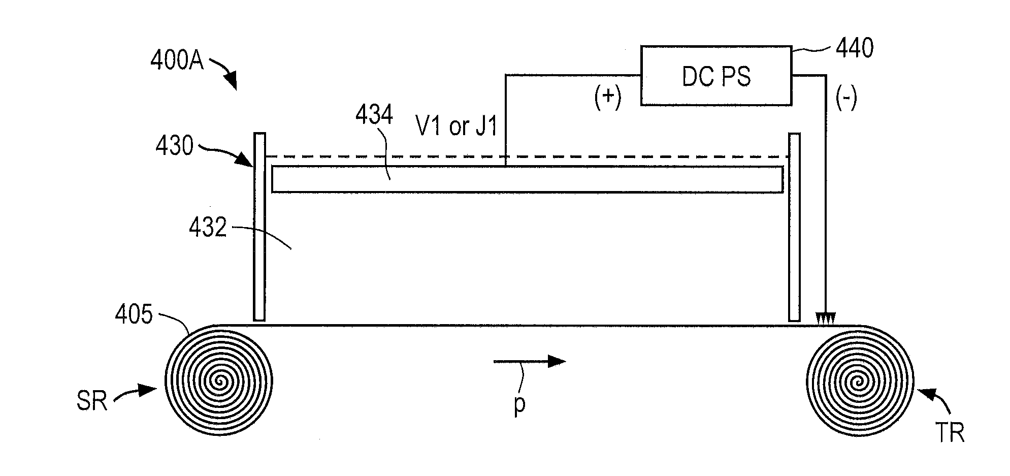
[0087]The Ga—Se solution used was comprised of GaCl3 and H2SeO3 with a pH between 1 and 2.5. The solution also included at least one of the following additive groups of (a): anti-oxidants, (b) anti-floculants, (c) surface-active compounds (d) ionic conductivity enhancers. Electroplating of the Ga—Se layer was conducted on a stainless steel substrate having an Indium terminated top metal layer. The electroplating was done in a batch mode and the cathode was titanium covered with IrO2. The deposition profile consisted of an applied constant voltage of 3.4 V between the anode and the cathode. The total deposition time was 60 sec. The Ga / Se ratio of the resulting film was 1.48. The deposited Ga—Se layers had a smooth and continuous surface with good adhesion properties. The values coefficient of variation (CV=STDEV / Mean Value) were 1.89% and 5.69% of Ga and Se respectively.

example 2

[0088]The Ga—Se solution used was comprised of GaCl3 and H2SeO3 with a pH between 1 and 2.5. The solution also included at least one of the following additive groups of (a): anti-oxidants, (b) anti-flocculants, (c) surface-active compounds (d) ionic conductivity enhancers. Electroplating of the Ga—Se layer was conducted on a stainless steel substrate having an Indium terminated top metal layer. The electroplating was done in a batch mode and the cathode was titanium covered with IrO2. This time a pulsed voltage was applied during plating. The applied potential was modulated between 3.4 V for 500 milliseconds and 2.2 V for 50 milliseconds for a total deposition time of 54 sec. The deposited Ga—Se layers had a smooth and continuous surface with good adhesion properties. The Ga / Se ratio deposited in this case is 1.6. The coefficient of variation (CV=STDEV / Mean Value) are 1.71% and 3.78% of Ga and Se respectively.

[0089]Although the embodiments have been particularly described, it should...


PUM

PropertyMeasurementUnit
Electric potential / voltageaaaaaaaaaa
Current densityaaaaaaaaaa

Abstract

The embodiment described herein relate to pulse electroplating methods and solutions.

Description

CROSS-REFERENCE TO RELATED APPLICATIONS[0001]This application is a continuation-in-part of U.S. patent application Ser. No. 13 / 347,540 filed Jan. 10, 2012, which is a continuation of U.S. patent application Ser. No. 12 / 143,609 filed Jun. 20, 2008 (now U.S. Pat. No. 8,092,667), and is a continuation-in-part of U.S. patent application Ser. No. 13 / 306,863 filed Nov. 29, 2011, which is a continuation of U.S. patent application Ser. No. 12 / 123,372 filed May 19, 2008 (now U.S. Pat. No. 8,066,865), and is a continuation-in-part of U.S. patent application Ser. No. 12 / 121,687 filed May 15, 2008, and the entire contents of these applications are incorporated herein by reference.BACKGROUND[0002]1. Field of the Art[0003]This application relates to electroplating methods and solutions and, more particularly, to methods and electroplating solution chemistries for electrodeposition of Group IIIA-VIA layers on a conductive surface for solar cell applications.[0004]2. Description of the Related Art[...

Claims


Application Information

Patent Timeline
IPC IPC(8): C25D3/56C25D5/18
CPCC25D3/56C25D5/18C25D3/54C25D5/10H01L31/0322H01L21/02628C25D7/126Y02E10/541H01L21/02568H01L21/02614H01L31/03923C25D5/611Y02P70/50
Inventor KLEIMAN-SHWARSCTEIN, ALANAKSU, SERDARPINARBASI, MUSTAFA
Owner SOLOPOWER
Why Eureka
Try Eureka