Coil inductor for on-chip or on-chip stack

a technology of inductor and coil, applied in the field of semiconductor devices, can solve the problems of reducing the effective inductance, and unable to achieve sufficient high inductance with a spiral inductor

Inactive Publication Date: 2013-05-09
IBM CORP
View PDF7 Cites 17 Cited by
  • Summary
  • Abstract
  • Description
  • Claims
  • Application Information

AI Technical Summary

Benefits of technology

[0013]According to another aspect of the invention, a method is provided for making an element having a coil inductor thereon, the element configured for connection within a microelectronic package. Such method can include forming a continuous coil inductor on an element including at least one of semiconductor, glass or ceramic material, the element having first and second opposed surfaces and a thickness between the first and second surfaces of less than 1000 microns. The coil inductor can include a plurality of conductive vias extending in a direction of the thickness, first electrically conductive li

Problems solved by technology

Heretofore, on-chip inductor structures have suffered from insufficient inductance per unit area of the surface of the microelectronic element.
The magnetic flux in a spiral inductor extends in a direction perpendicular to the planar surfaces of the ch

Method used


Image

  • Coil inductor for on-chip or on-chip stack
  • Coil inductor for on-chip or on-chip stack
  • Coil inductor for on-chip or on-chip stack

Examples


Embodiment Construction

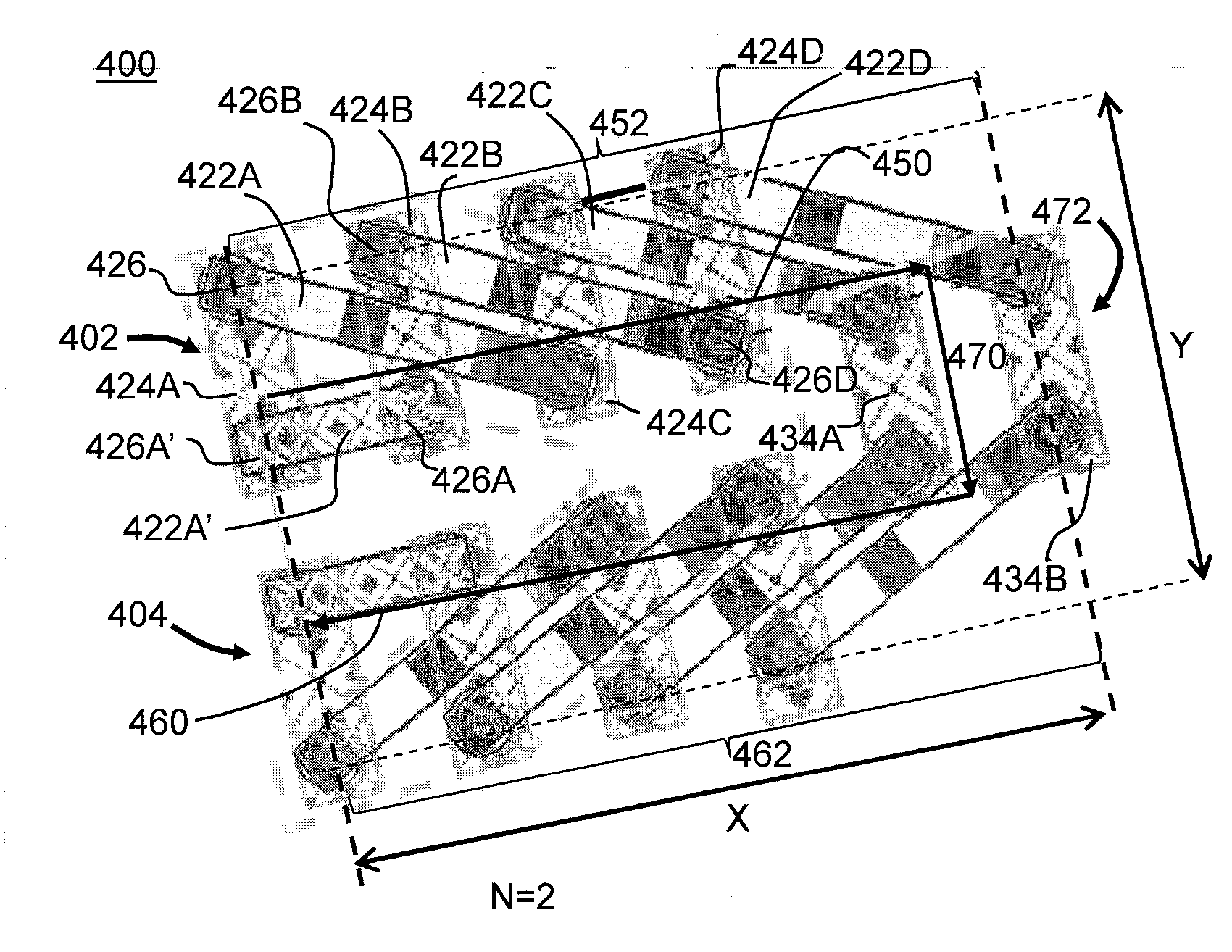
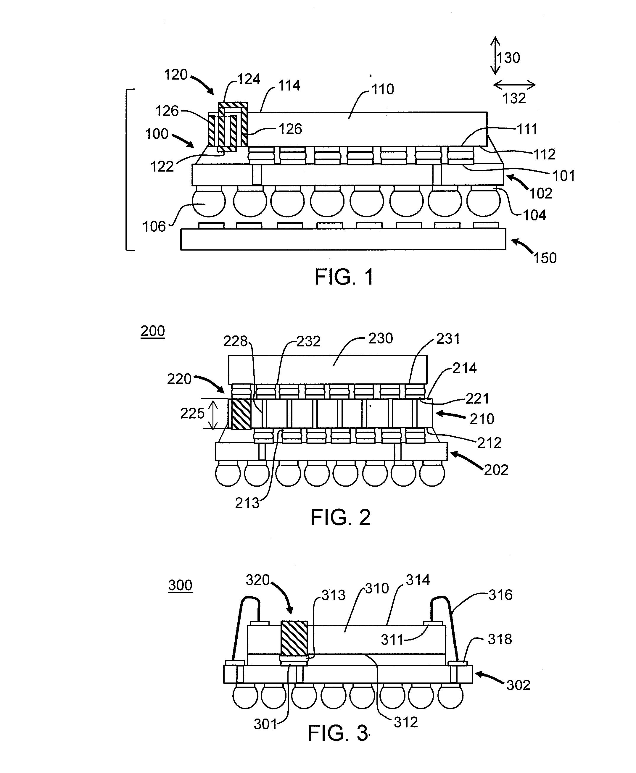
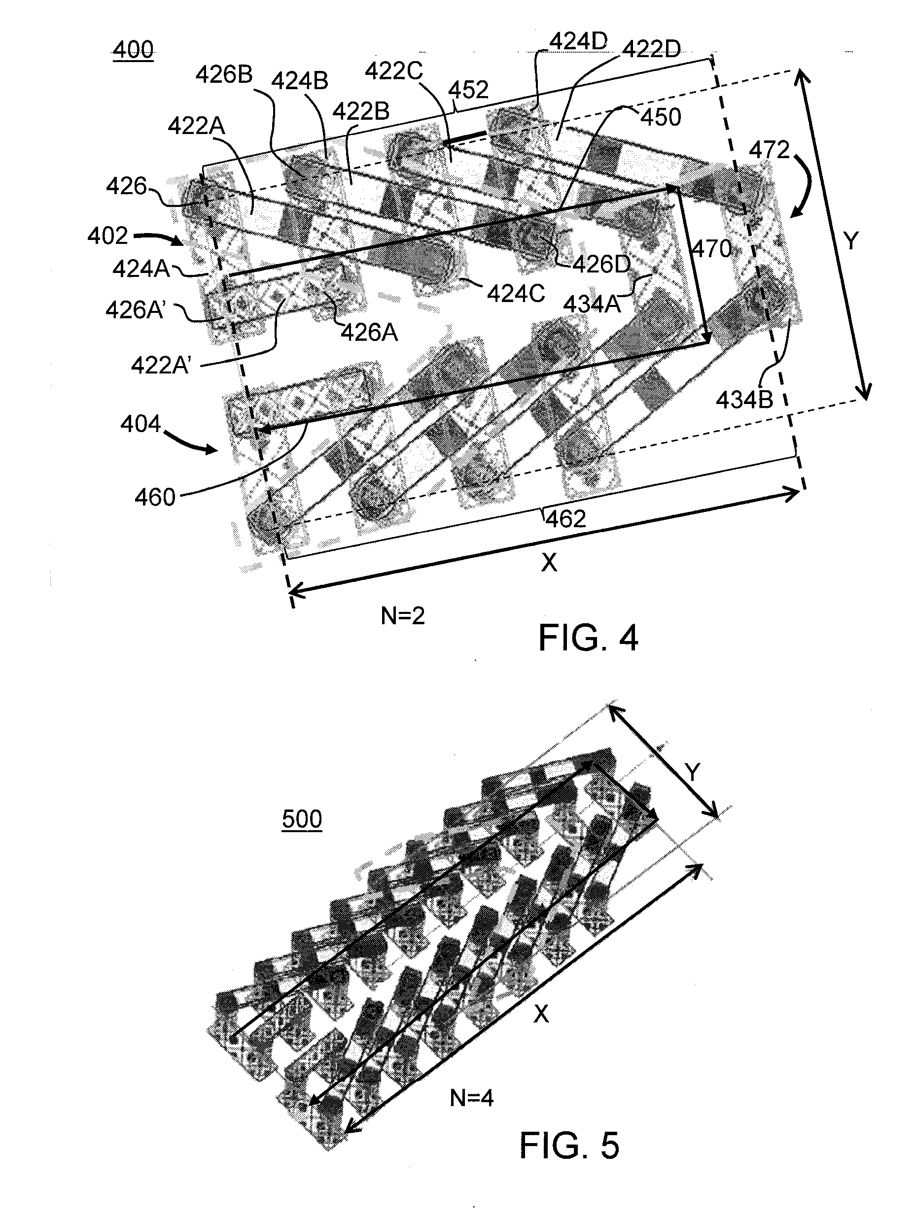
[0024]Accordingly, a coil inductor structure is provided which can be fabricated on a microelectronic element such as a semiconductor chip, or interconnection element such as a semiconductor, glass or ceramic interposer element, which when energized has magnetic flux extending in a direction parallel to first and second opposed surfaces of the microelectronic or interconnection element, and whose peak magnetic flux is disposed between the first and second surfaces. The coil inductor can include first conductive lines extending along the first surface of the microelectronic or interconnection element, second conductive lines extending along the second surface of the microelectronic or interconnection element, and a plurality of conductive vias, e.g., through silicon vias, extending in a direction of a thickness of the microelectronic or interconnection element. Embodiments of the invention further provide a coil inductor which is configured to couple the magnetic flux directly betwee...


PUM


Abstract

A coil inductor and buck voltage regulator incorporating the coil inductor are provided which can be fabricated on a microelectronic element such as a semiconductor chip, or on an interconnection element such as a semiconductor, glass or ceramic interposer element. When energized, the coil inductor has magnetic flux extending in a direction parallel to first and second opposed surfaces of the microelectronic or interconnection element, and whose peak magnetic flux is disposed between the first and second surfaces. In one example, the coil inductor can be formed by first conductive lines extending along the first surface of the microelectronic or interconnection element, second conductive lines extending along the second surface of the microelectronic or interconnection element, and a plurality of conductive vias, e.g., through silicon vias, extending in direction of a thickness of the microelectronic or interconnection element. A method of making the coil inductor is also provided.

Description

BACKGROUND OF THE INVENTION[0001]The present invention relates to semiconductor devices and their manufacture, and more specifically to a structure and method of making a coil inductor on a semiconductor chip, on an interconnection device, or on a plurality of stacked semiconductor chips.[0002]For certain applications it is desirable to provide an inductor having a relatively large inductance value on a microelectronic element such as a semiconductor integrated circuit chip, or on an interconnection element such as an interposer for electrical connection with a microelectronic element in a microelectronic package. A relatively large inductance value is needed when the inductor is used in a power supply voltage regulator, such as a buck voltage regulator commonly used to step up or step down a voltage from one direct current (DC) supply voltage to another. Heretofore, buck voltage regulators have been implemented as devices mounted to a circuit board rather than on microelectronic el...

Claims


Application Information

Patent Timeline
IPC IPC(8): G05F1/10H01L21/02H01F5/00H01L27/06
CPCH01L23/49822H01L2924/01322H01L23/645H01L28/10H01L2224/16225H01L2224/32225H01L2224/48227H01L2224/73265H01L2924/15311H01L23/5227H01F17/0013H01F2017/0086H01L2924/30107H01F41/005H01L2924/00
Inventor SHAPIRO, MICHAEL J.CARPENTER, GARY D.DRAKE, ALAN J.GORDIN, RACHELSPROGIS, EDMUND J.
Owner IBM CORP
Why Eureka
Try Eureka