

Anistropic semiconductor nanoparticles
a technology of anisotropic semiconductors and nanoparticles, which is applied in the field of nanomaterials, can solve the problems of the lower fluorescence quantum efficiency of spherical nanocrystals, the shape of nanorods (nrs), and the comparison of spherical nanocrystals to spherical nanocrystals, so as to reduce the overlap of electron-holes, reduce the fluorescence quantum efficiency, and increase the delocalization
- Summary
- Abstract
- Description
- Claims
- Application Information
AI Technical Summary
Benefits of technology
Problems solved by technology
Method used
Image

Examples
example a1
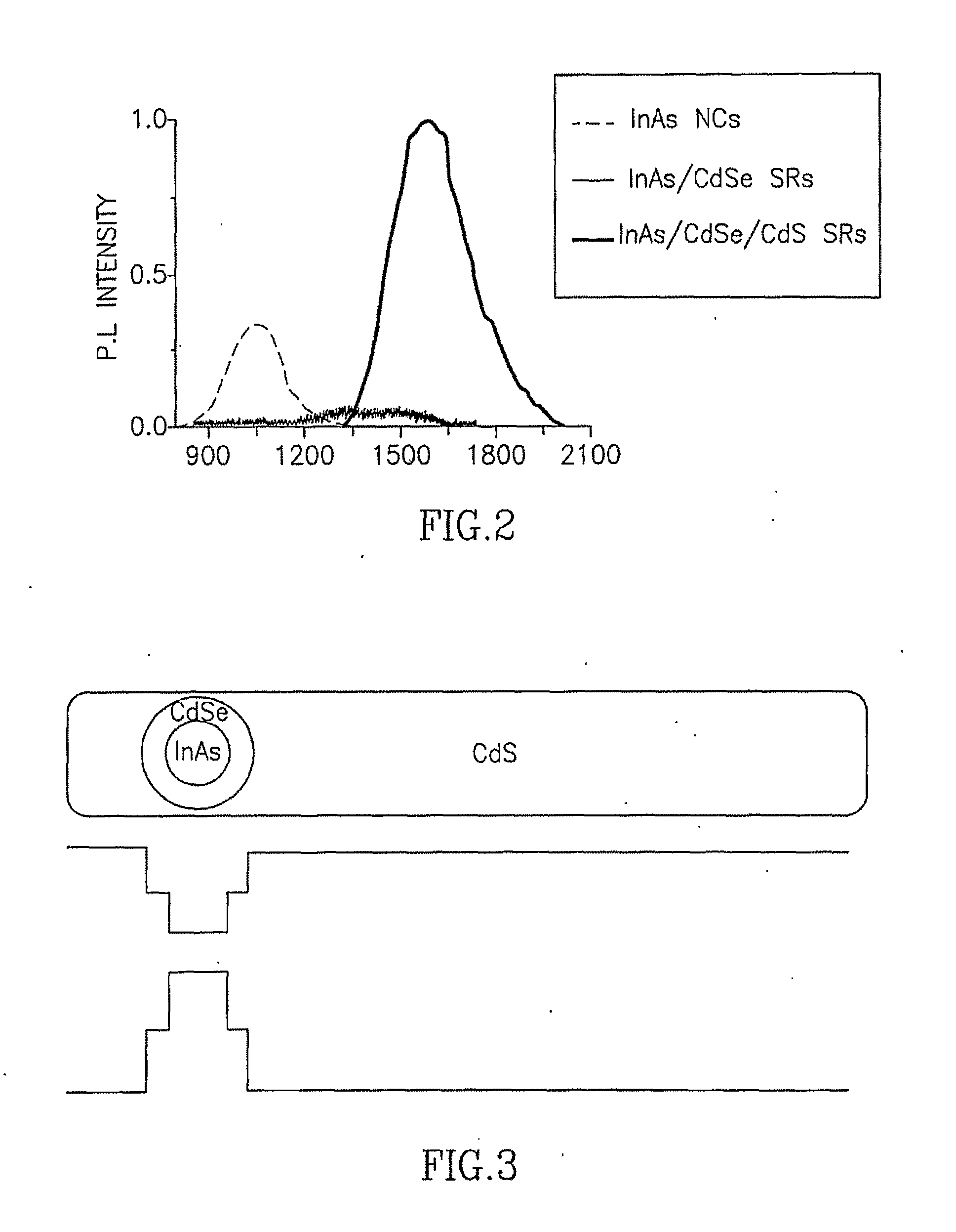
InAs / CdSe / CdS
[0261]The synthesis of InAs / CdS SR systems according to the present invention was performed according to the seeded-growth approach, by rapidly injecting a mixture of InAs NCs, grown according to literature [36] and sulfur precursor into a hot solution of cadmium precursor and two phosphonic acids in tri-n-octylphosphine oxide.
[0262]As demonstrated in FIG. 2, in which the emission of InAs NCs and of InAs / CdS SR is shown, the growth of the CdS shell directly on top of the InAs seeds induced a large red shift (from 970 nm to 1500 nm) accompanied by a broadening of the emission peak and by a significant reduction of its intensity. This reduction can be attributed to formation of traps and intermediate states in the InAs / CdS interface as a results of large lattice mismatch between the two materials (6.058 Å for InAs and 5.832 Å for CdS fcc structures). To overcome the lattice mismatch problem, an intermediate layer was constructed on top of the core, forming a core-shell st...
example a2
InAs / CdSe / ZnSe / CdS
[0269]In this example, an additional shell of ZnSe was grown on the InAs / CdSe core / shell, using a layer by layer (LBL) method. Formation of the second shell was aimed at increasing the potential barrier, thus leading to a decrease in the red shift of the emission (from 1600 nm to 1400 nm) and enable further control of the band gap energy. Controlling the shift is achieved by changing the thickness of the different shells (FIG. 8).
example a3
InP / ZnSe / CdS
[0270]Another kind of combination between II-VI and III-V materials was achieved by using InP as core. The band gap of bulk InP (1.34 eV) is higher than the InAs (0.35 eV), resulting a shorter wavelength emission, and enabled to reach the visible-NIR spectrum range (500-900). This range is of high interest for lighting, displays and biological applications. InP / ZnSe quantum dots were synthesized by a drop-wise addition of Zn and Se precursors on the pre-synthesized InP cores. This was done either by alternating injections of the Zn and the Se precursors (using the layer-by-layer method) or by a continuous injection of a mixture of both precursors. Another possible method for achieving InP / ZnSe core / shell was by seeded growth of the ZnSe shell, in which the InP cores were mixed with the Se precursor and injected rapidly to a heated mixture of the Zn precursor and ligands (long chained amines, phosphineoxides, etc.)
[0271]The core / shell seeds are injected to the growth solu...
PUM
 Abstract
Description
Claims
Application Information