Multilayer ceramic electronic component

Active Publication Date: 2013-05-16
SAMSUNG ELECTRO MECHANICS CO LTD
View PDF1 Cites 7 Cited by
  • Summary
  • Abstract
  • Description
  • Claims
  • Application Information

AI Technical Summary

Benefits of technology

The present patent is about improving the sealing properties of a chip in a multilayer ceramic electronic component to enhance its reliability. The technical effect of this invention is better protection and insulation of the chip, resulting in more reliable performance of the overall electronic component.

Problems solved by technology

However, in the case in which a content of glass in the external electrode paste is insufficient, chip sealing properties may be defective.
In the case an excessive amount of glass is added to the external electrode paste in order to complement the chip sealing properties, a defect such as a plating defect may occur due to the elution of the glass to a surface.
Particularly, in accordance with the thinning of the external electrode, it is difficult to implement a desired level of density, and the possibility that a defect will occur due to a deficiency or excess of glass, owing to high temperature behavior characteristics of the glass, may be increased.
In addition, in a small-sized multilayer ceramic electronic component in which a coating thickness of the external electrode is thin, a thickness of the external electrode at a corner portion maybe especially thin, such that corner coverage performance is low.

Method used


Image

  • Multilayer ceramic electronic component
  • Multilayer ceramic electronic component
  • Multilayer ceramic electronic component

Examples


Embodiment Construction

[0039]Embodiments of the present invention may be modified in many different forms and the scope of the invention should not be limited to the embodiments set forth herein. Rather, these embodiments are provided so that this disclosure will be thorough and complete, and will fully convey the concept of the invention to those skilled in the art. In the drawings, the shapes and dimensions may be exaggerated for clarity, and the same reference numerals will be used throughout to designate the same or like components.

[0040]Embodiments of the present invention will now be described in detail with reference to the accompanying drawings.

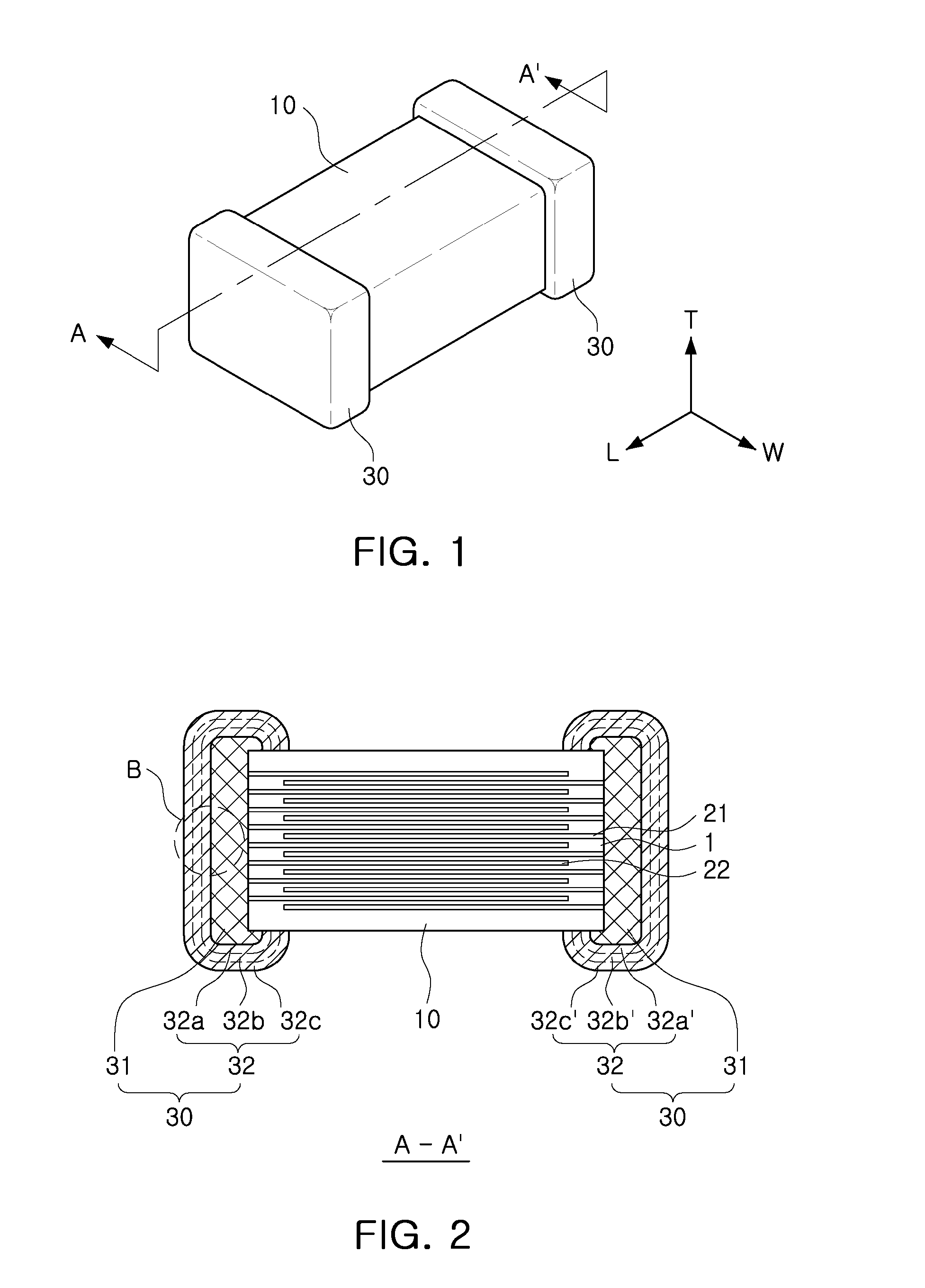
[0041]FIG. 1 is a perspective view schematically showing a multilayer ceramic capacitor according to an embodiment of the present invention.

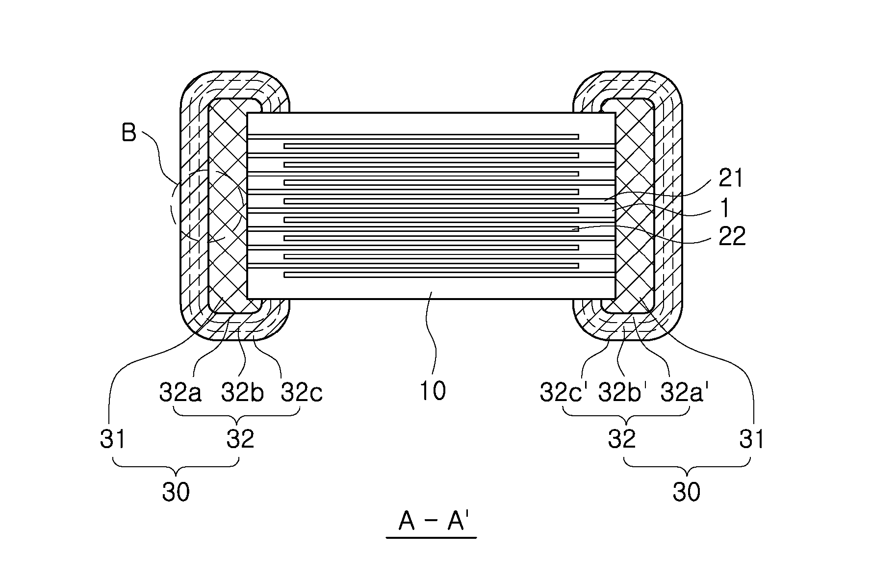
[0042]FIG. 2 is a cross-sectional view of line A-A′ of FIG. 1.

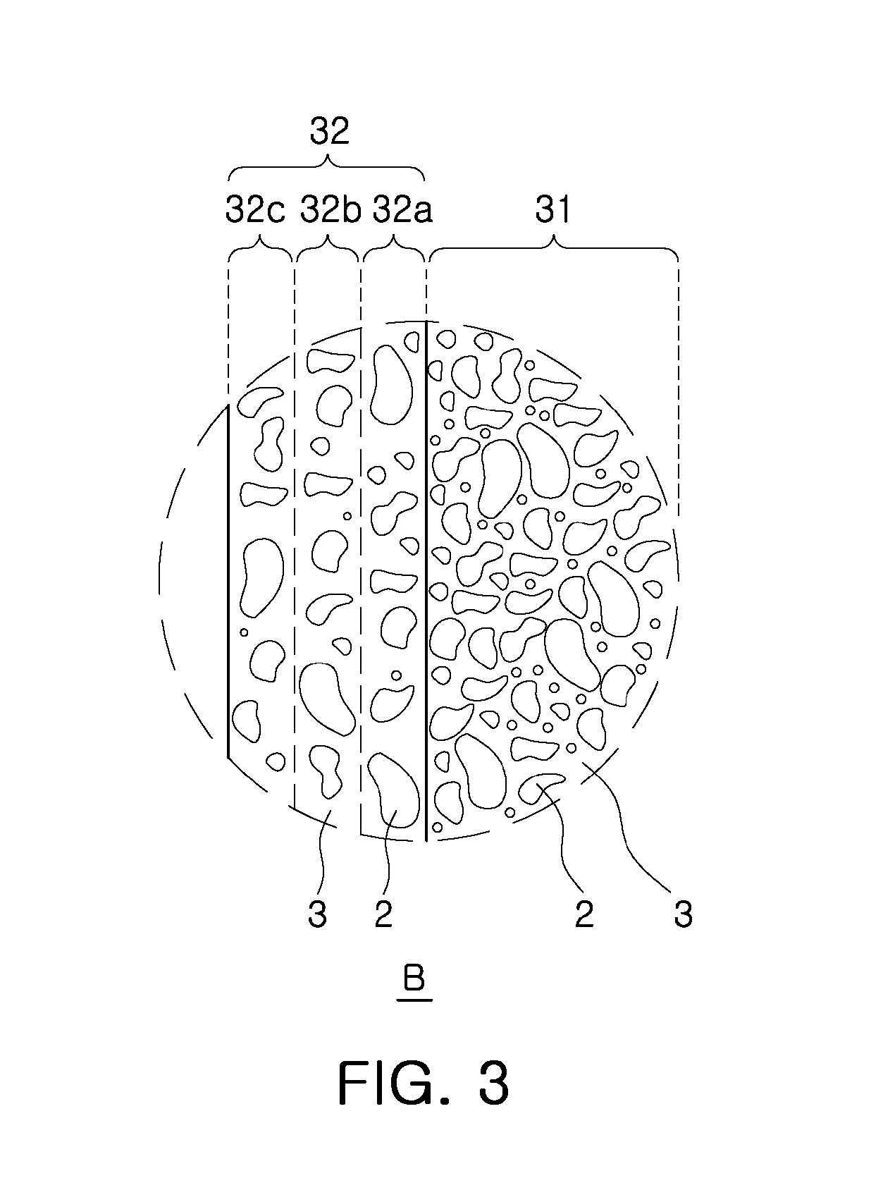
[0043]FIG. 3 is an enlarged view of part B of FIG. 2.

[0044]Referring to FIGS. 1 to 3, the multilayer ceramic electronic component according to the embodiment...


PUM

PropertyMeasurementUnit
Temperatureaaaaaaaaaa
Fractionaaaaaaaaaa
Percent by massaaaaaaaaaa

Abstract

There are provided a multilayer ceramic electronic component and a method of manufacturing the same. The multilayer ceramic electronic component includes: a ceramic body including a dielectric layer; first and second internal electrodes disposed within the ceramic body to face each other, while having the dielectric layer interposed therebetween; and first external electrodes electrically connected to first and second internal electrodes and second external electrodes formed on the first external electrodes, wherein the first and second external electrodes include a conductive metal and a glass, and when the second external electrodes are divided into three equal parts in a thickness direction, an area of the glass in central parts thereof with respect to an area of the central parts is 30 to 80%. Therefore, sealing properties of a chip is improved, whereby a multilayer ceramic electronic component having improved reliability may be implemented.

Description

CROSS-REFERENCE TO RELATED APPLICATIONS[0001]This application claims the priority of Korean Patent Application No. 10-2011-0117398 filed on Nov. 11, 2011, in the Korean Intellectual Property Office, the disclosure of which is incorporated herein by reference.BACKGROUND OF THE INVENTION[0002]1. Field of the Invention[0003]The present invention relates to a multilayer ceramic electronic component having improved reliability by improving sealing properties of a chip.[0004]2. Description of the Related Art[0005]In accordance with the recent trend for the miniaturization of electronic products, demand for multilayer ceramic electronic components having a small size and high capacitance has increased.[0006]In accordance with the demand for multilayer ceramic electronic components having a small size and high capacitance, an external electrode of the multilayer ceramic electronic component has also been thinned.[0007]An external electrode paste may include a conductive metal such as copper...

Claims


Application Information

Patent Timeline
IPC IPC(8): H01G4/30H01B1/02H01G13/00
CPCH01G4/30H01B3/12Y10T29/417H01G4/2325H01G4/12
Inventor PARK, MYUNG JUNKWON, SANG HOONKIM, CHANG HOONGU, HYUN HEEPARK, JAE YOUNGCHOI, DA YOUNGLEE, KYU HAJEON, BYUNG JUN
Owner SAMSUNG ELECTRO MECHANICS CO LTD
Why Eureka
Try Eureka