Band-pass filter module and module substrate

a filter module and filter substrate technology, applied in the direction of waveguide type devices, electrical apparatus contructional details, printed circuit non-printed electric components association, etc., can solve the problems of insufficient proposals, filter is more susceptible to deterioration of filter characteristics, etc., and achieve satisfactory filter characteristics.

Active Publication Date: 2013-05-16
TDK CORPARATION
View PDF8 Cites 7 Cited by
  • Summary
  • Abstract
  • Description
  • Claims
  • Application Information

AI Technical Summary

Benefits of technology

[0032]According to the present invention, satisfactory filter characteristics can be

Problems solved by technology

As such, when a filter including an LC resonator, for example, is to be reduced in height, the filter is more susceptible to deteriorations in filter characteristics, caused by stray capacitance and undesired electromagnetic coupling, such as a lower Q-value due to an inductor included in the filter which is pl

Method used


Image

  • Band-pass filter module and module substrate
  • Band-pass filter module and module substrate
  • Band-pass filter module and module substrate

Examples


first embodiment

[0062]A BPF module according to a first embodiment of the present invention comprises a chip-like BPF (bandpass filter, hereinafter referred to as the “BPF chip” or “filter chip” or simply as the “chip”), and a PCB (Printed Circuit Board) for mounting this BPF chip. The PCB comprises a PWB (Printed Wiring Board) which serves as a mounting board, a variety of electronic parts mounted thereon, and circuit elements formed therein such as conductor lines and terminal electrodes for connection, vias, and the like.

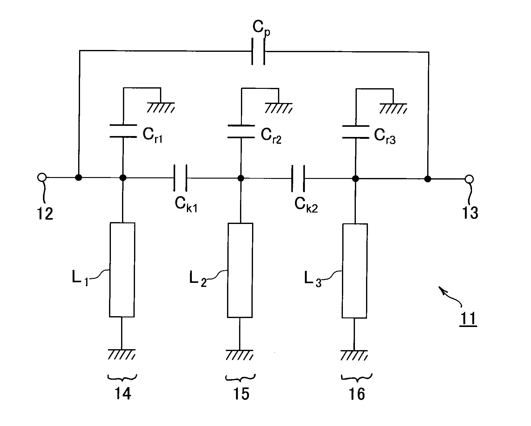
[0063]As shown in FIG. 1, a BPF chip 11 comprises three resonators 14, 15, 16 connected in order between an input terminal 12 and an output terminal 13 for forming a predetermined pass band; coupling capacitors (inter-stage capacitors) Ck1 and Ck2 for coupling these resonators 14-16; a bypass capacitor (bypass condensor) Cp connected between the input terminal 12 and output terminal 13 in parallel with the resonators 14-16. Each of the resonators 14-16 is an LC parallel resonato...

second embodiment

[0091]FIG. 21 is a circuit diagram showing a BPF chip which may be employed in a module according to a second embodiment of the present invention. While the first embodiment employs a BPF which comprises three resonators, this embodiment employs a BPF chip 101 which comprises four resonators disposed in a laminated board (LTCC board), including a first resonator 114, a second resonator 115, a third resonator 116, and a fourth resonator 117 connected in order between an input terminal 12 and an output terminal 13, as shown in FIG. 21.

[0092]Also, this embodiment is similar to the first embodiment in that middle-stage resonators, i.e., the second resonator 115 and third resonator 116 are disposed in the chip middle zone, and that these middle-stage resonators 115, 116 are made up of inductor electrodes and capacitor electrodes which are formed on wiring layers in a lower portion of the chip 101.

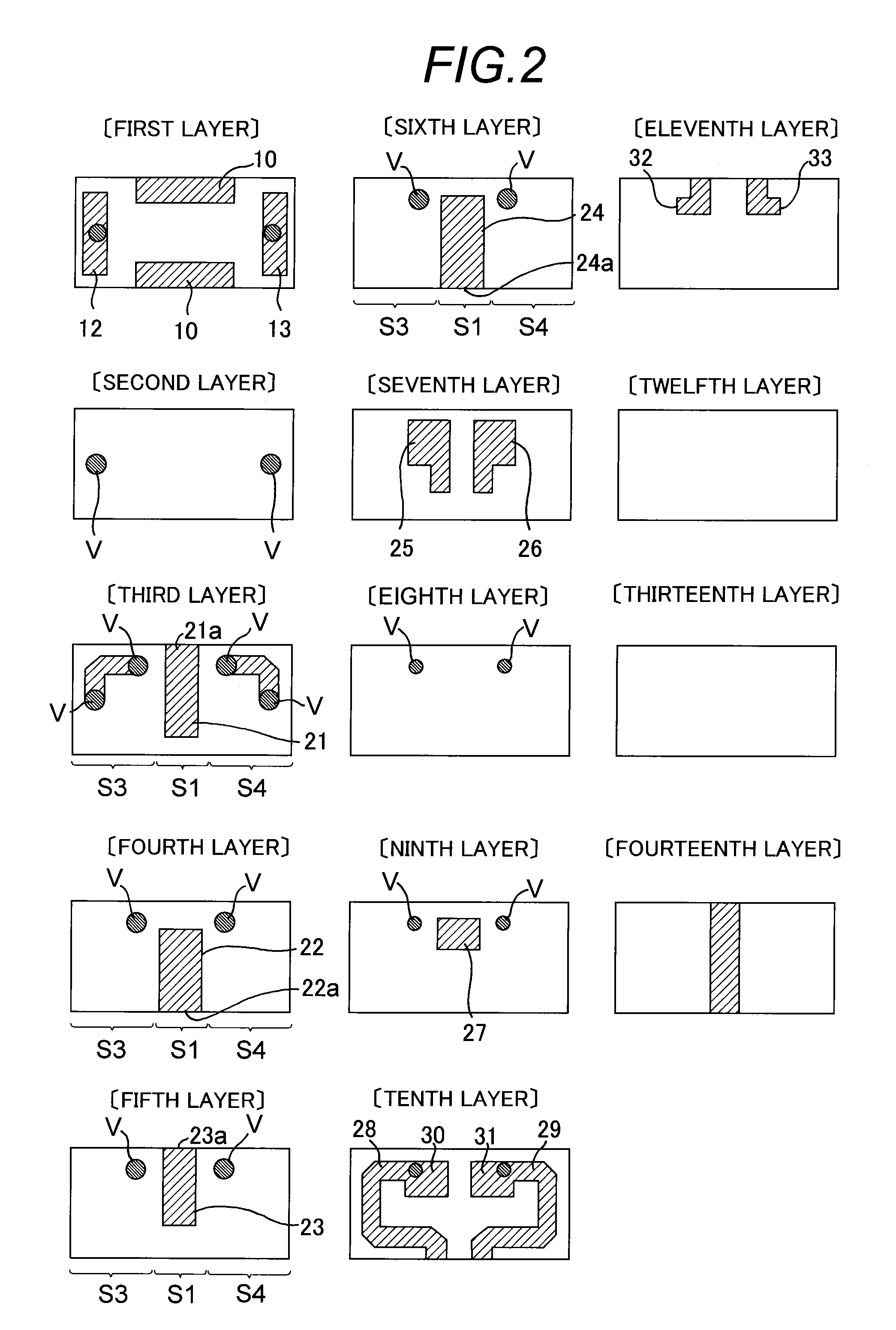
[0093]Conductor patterns on each wiring layer are formed as shown in FIG. 22. As shown in FI...

third embodiment

[0095]Further, while the first and second embodiments employ a laminated board for forming a filter chip, the filter chip can be alternatively implemented by a so-called thin-film chip which involves the lamination using a thin-film technology (vapor deposition method).

[0096]In a third embodiment of the present invention, such a thin-film chip is mounted on the surface of the PCB 70 instead of the chip 11 of the first embodiment. As shown in FIG. 23, this thin-film chip 201 is fabricated by alternately depositing electrode films and insulating films using a vapor deposition method such as sputtering, vapor deposition, and the like to form each wiring layer. Also, the chip 201 is a filter which comprises three (first through third) resonators 14-16, like the first embodiment.

[0097]As shown in FIG. 24, the chip 201 has ten wiring layers in this example. Like the chip in the first embodiment, an input terminal 12, an output terminal 13, and ground terminals 10 are each disposed on the ...


PUM


Abstract

A bandpass filter module includes a mounting board and a BPF chip mounted on a surface thereof. The BPF chip includes three or more resonators; a first-stage resonator located closest to an input terminal, a final-stage resonator located closest to an output terminal, and a middle-stage resonator connected between the first-stage and the final-stage resonators and located in a chip middle zone. The mounting board includes an area overlapping with the chip middle zone, viewed in plan, defining a ground-free space in which no ground electrode is disposed. The ground-free space is formed at least from the surface of the mounting board to a depth position at which a topmost internal wiring layer is located. The middle-stage resonator is prevented from being coupled to ground electrodes on the mounting board and from a lower Q-value and increased insertion loss.

Description

TECHNICAL FIELD[0001]The present invention relates to a bandpass filter module and a module board, and more particularly, to techniques for avoiding the influence (deteriorations in filter characteristics) exerted by a ground electrode, a shield case, and the like disposed on a mounting board in a modular structure for mounting a bandpass filter in the form of chip on the surface of the mounting board.BACKGROUND ART[0002]As electronic devices have been increasingly reduced in size and height and provided with more functions, electronic parts which comprise the devices are highly required to be reduced in size and height (thickness), increased in functionality and integration. For example, a bandpass filter (hereinafter sometimes referred to as the “BPF”) employed in a communication device such as a portable phone, a wireless LAN device, and the like, plays an important role of selecting frequencies while removing unwanted waves for the communication device. For responding to such re...

Claims


Application Information

Patent Timeline
IPC IPC(8): H05K1/18H05K1/11H03H7/01
CPCH01P1/20345H05K1/0243H03H7/1708H03H7/1775H03H7/0115H05K1/181H05K1/115H05K1/18H03H7/0123H03H2001/0085H05K1/0224H05K1/11
Inventor TOMAKI, SHIGEMITSUTSUYA, YOSHIKAZUTANAKA, MASAMICHIABE, ISAO
Owner TDK CORPARATION
Why Eureka
Try Eureka