Liquid crystal device and electronic apparatus

a liquid crystal device and electronic equipment technology, applied in non-linear optics, instruments, optics, etc., can solve problems such as display defects, display unevenness or burn-in, and display defects caused by eccentric locations of positive or negative ionic impurities, and achieve high reliability and reduce display defects

Active Publication Date: 2013-05-23
SEIKO EPSON CORP
View PDF7 Cites 21 Cited by
  • Summary
  • Abstract
  • Description
  • Claims
  • Application Information

AI Technical Summary

Benefits of technology

[0011]With such a configuration, a first electric field is generated between the pixel electrodes and the first connection line layer to which the first potential lower than the common potential is applied. In addition, a second electric field is generated between the pixel electrodes and the second connection line layer to which the second potential higher than the common potential of the first substrate is applied. The direction of the second electric field with respect to the direction of the first electric field is a reverse direction, the second connection line layer is provided to overlap with at least a part of the first connection line layer in the plan view, and thus the first electric field generated between the first connection line layer and the pixel electrode is weakened. Accordingly, the positive ionic impurities in the liquid crystal layer attracted by the first electric field generated between the first connection line layer and the pixel electrodes are reversed by the second electric field generated between the second connection line layer and the pixel electrodes, and may be dispersed in the liquid crystal layer. Accordingly, a display defect such as display unevenness or burn-in caused by partial eccentric location of positive ionic impurities is reduced, and it is possible to provide the liquid crystal device having high reliability with a stable display state kept.Application Example 2
[0017]Alternating current potential with different polarities is applied to the pixel electrodes with the common potential considered as a reference, and on average, the potential is substantially the common potential. With such a configuration, the third connection line layer to which the common potential is applied is provided between the second connection line layer and the pixel electrodes, and thus the intensity of the second electric field generated between the pixel electrodes and the second connection line layer is increased as compared with a case where the third connection line layer is not provided. That is, it is possible to more effectively disperse the positive or negative ionic impurities which become a factor for causing display defects in the liquid crystal layer.Application Example 5
[0043]With such a configuration, it is possible to provide the electronic apparatus in which display defects caused by the eccentric location of the positive or negative ionic impurities are reduced and which has high reliability.

Problems solved by technology

However, when ionic impurities are included in the liquid crystal layer, the insulating property is decreased in the whole liquid crystal layer or parts thereof, and thus, a desired driving voltage is not applied.
Accordingly, a display defect such as display unevenness or burn-in may occur.
For example, when the potential-applied connection line is closer to the pixel electrode than the ionic impurity adsorption electrode, it is thought that ionic impurities in liquid crystal are eccentrically located in the display area of attracting the ionic impurities by an electric field generated between the connection line and the pixel electrode, and the ionic impurities either cannot be adsorbed at all or cannot be adsorbed efficiently even when potential is applied to the ionic impurity adsorption electrode.
That is, even when the ionic impurity adsorption electrode is disposed on the outside of the display area of the active matrix substrate, there is a problem that it may be difficult to obtain a desired effect.

Method used


Image

  • Liquid crystal device and electronic apparatus
  • Liquid crystal device and electronic apparatus
  • Liquid crystal device and electronic apparatus

Examples


first embodiment

[0062]In the embodiment, an active matrix type liquid crystal device provided with thin film transistors as switching elements of pixels will be described by way of example. The liquid crystal device may be appropriately used, for example, as an optical modulation element (a liquid crystal light valve) of a projection type display device (a liquid crystal projector) to be described later.

Liquid Crystal Device

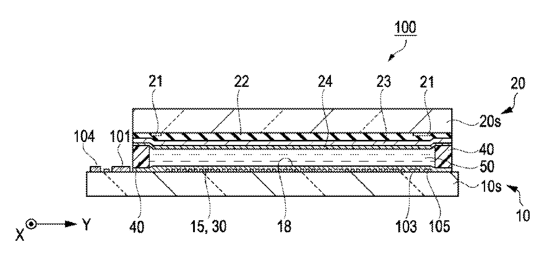
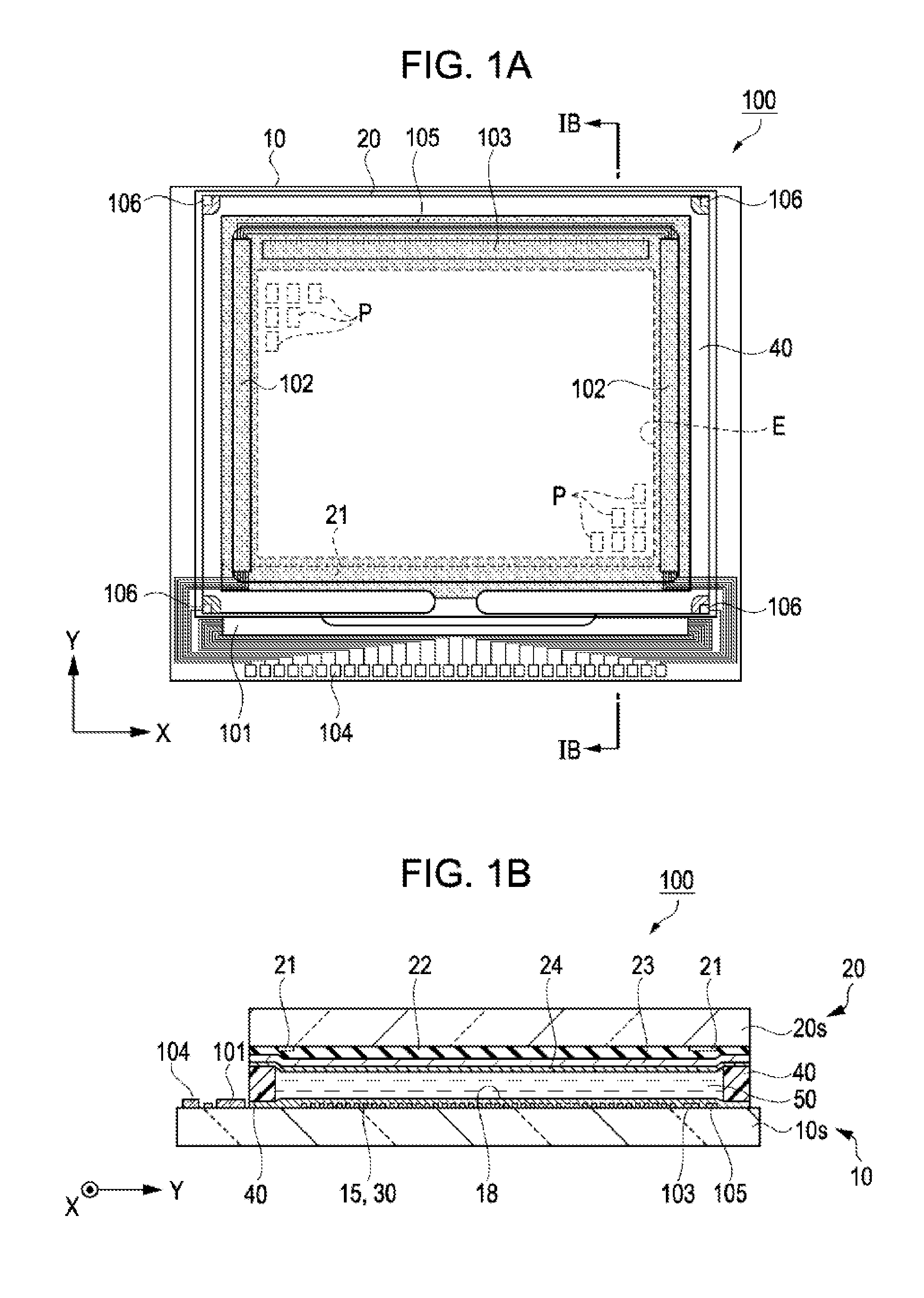
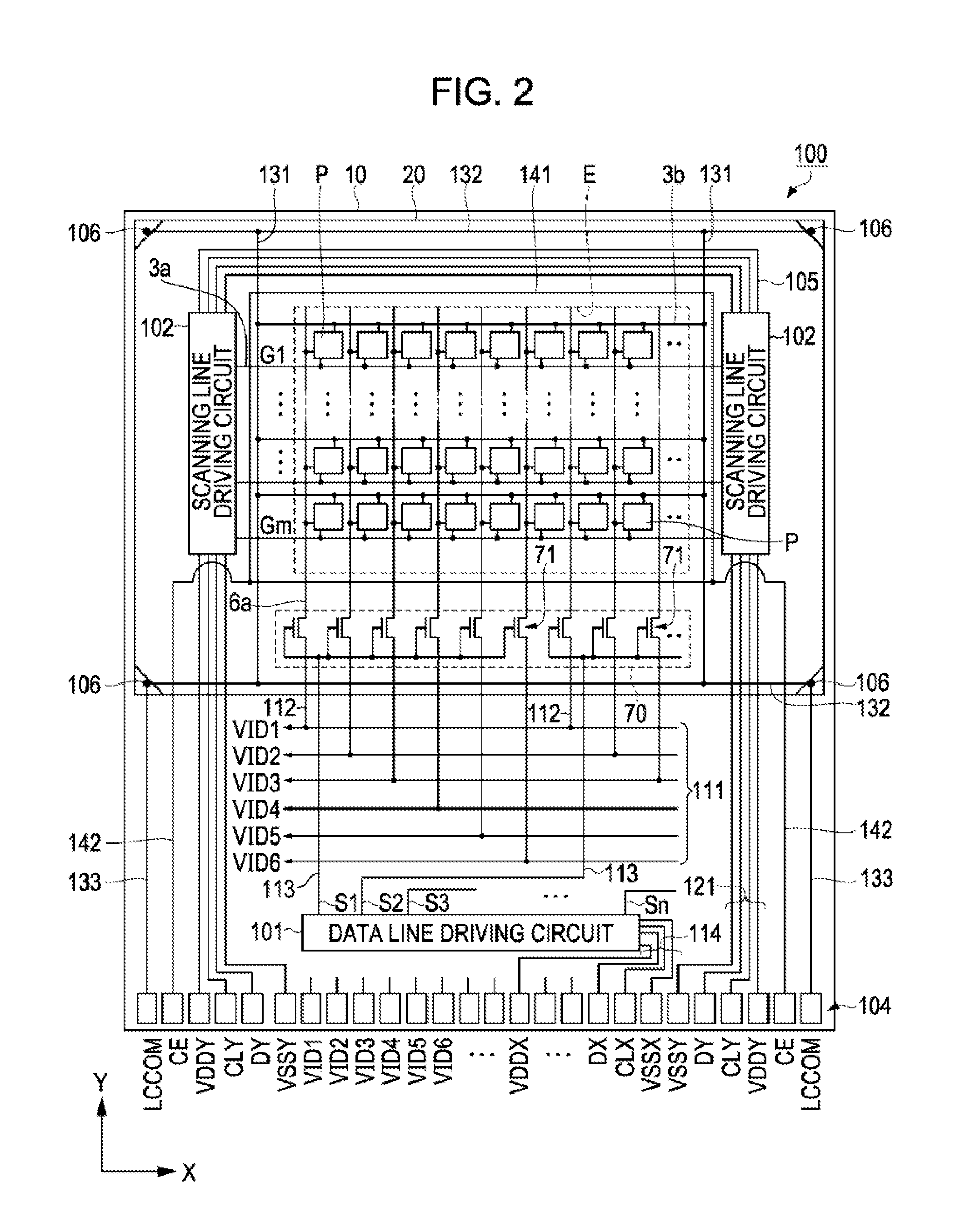
[0063]First, a liquid crystal device of the embodiment will be described with reference to FIG. 1A to FIG. 3. FIG. 1A is a schematic plan view illustrating a configuration of the liquid crystal device, FIG. 1B is a schematic cross-sectional view illustrating a structure of the liquid crystal device taken along the line IB-IB of FIG. 1A, FIG. 2 is a circuit diagram illustrating an electrical configuration of the liquid crystal device, FIG. 3 is an equivalent circuit diagram illustrating an electrical configuration of a pixel, and FIG. 4 is a schematic cross-sectional view illustr...

example 1

[0116]FIG. 7A is a schematic cross-sectional view illustrating a connection line structure in an element substrate of Example 1, and FIG. 7B is a schematic cross-sectional view illustrating a modification example in disposition of a peripheral electrode and a connection line of Example 1.

[0117]As shown in FIG. 7A, in Example 1, in the connection line layer 12 of the peripheral area E3, a scanning line driving circuit connection line 121s (hereinafter, referred to as a positive potential connection line 121s) to which the reference potential (VSSY) is supplied (applied), and a scanning line driving circuit connection line 121d to (hereinafter, referred to as a positive potential connection line 121d) to which the driving potential (VDDY) is supplied (applied) are disposed. A connection line 131 for supplying (applying) the common potential (LCCOM) to the connection line layer 13 between the positive potential connection line 121s and the dummy pixel area E2 is disposed. In the same l...

example 2

[0125]FIG. 9 is a schematic cross-sectional view illustrating a connection line structure in an element substrate of Example 2 shown in FIG. 9. In Example 2, a range where the peripheral electrode 141 is provided is different from that of Example 1. Specifically, as shown in FIG. 9, the peripheral electrode 141 of Example 2 is formed in the same layer as the pixel electrode 15 such that the positive potential connection lines 121s and 121d provided in the connection line layer 12 overlaps with the connection line 131 provided in the connection line layer 13 in the plan view.

[0126]According to Example 2, the first electric field generated between the positive potential connection lines 121s and 121d and the pixel electrode 15 is blocked, and it is possible to raise the intensity of the second electric field generated between the peripheral electrode 141 and the pixel electrode 15. By the direct current potential applied to the peripheral electrode 141, one of the positive or negative...


PUM

PropertyMeasurementUnit
transmittanceaaaaaaaaaa

Abstract

A liquid crystal device includes a positive potential connection line as a first connection line layer to which a first potential lower than a common potential is applied, between a pixel area and a seal member in the plan view, and a peripheral electrode as a second connection line layer that is provided between the positive potential connection line and a liquid crystal layer, is provided to overlap with at least a part of the positive potential connection line in the plan view, and to which a second potential higher than the common potential is applied.

Description

BACKGROUND[0001]1. Technical Field[0002]The present invention relates to a liquid crystal device and an electronic apparatus provided with the liquid crystal device.[0003]2. Related Art[0004]A liquid crystal device has a liquid crystal layer having a positive or negative dielectric anisotropy interposed between a pair of substrates. For example, each electrode is formed on the pair of substrates, a driving voltage is applied between the electrodes with the liquid crystal layer interposed therebetween to change an alignment state of liquid crystal molecules constituting the liquid crystal layer by an electric field effect, and thus it is possible to optically modulate light input to the liquid crystal layer on the basis of an image signal. The liquid crystal layer has a thickness of, for example, several μm, and a high insulating property. However, when ionic impurities are included in the liquid crystal layer, the insulating property is decreased in the whole liquid crystal layer or...

Claims


Application Information

Patent Timeline
Patent Type & Authority Applications(United States)
IPC IPC(8): G02F1/1345G02F1/1339
CPCG02F1/13452G02F1/1339G02F2001/133388G02F2001/133337G02F1/1345G02F1/133337G02F1/133388
Inventor NAGASAWA, HITOYA
Owner SEIKO EPSON CORP
Why Eureka
Try Eureka