Method of manufacturing resonant transducer

a resonant transducer and manufacturing method technology, applied in the manufacture of electrical transducers, microelectromechanical systems, microstructural devices, etc., can solve the problems of difficult to accurately control the tensile strain of vibration beams, unduly varying sensitivity, and the inability to give high tensile strain vibration beams when thick, etc., to achieve high tensile strain and high accuracy

Active Publication Date: 2013-06-06
YOKOGAWA ELECTRIC CORP
View PDF7 Cites 8 Cited by
  • Summary
  • Abstract
  • Description
  • Claims
  • Application Information

AI Technical Summary

Benefits of technology

[0027]One of illustrative aspects of the present invention is to provide a resonant transducer having a vibration beam that is high in accuracy and is given high tensile strain.

Problems solved by technology

Furthermore, the sensitivity varies unduly unless the variation of this initial tensile strain is controlled.
In the epitaxial method, because of occurrence of defects and dislocations in the vibration beam 3, it is difficult to accurately control the tensile strain of the vibration beam 3 and the vibration beam 3 cannot be given high tensile strain when it is thick.
Furthermore, a wafer may be warped by tensile film stress that is caused by the impurity.
On the other hand, to form a vibration beam 3 that is thick and is given high tensile strain by a related-art diffusion method, the diffusion length needs to be increased, resulting in a long diffusion time.
Furthermore, in the epitaxial method, a vibration beam 3 that is thick in the height direction cannot be formed because the tensile strain decreases in the case where it is thicker than about 5 μm.

Method used


Image

  • Method of manufacturing resonant transducer
  • Method of manufacturing resonant transducer
  • Method of manufacturing resonant transducer

Examples


Embodiment Construction

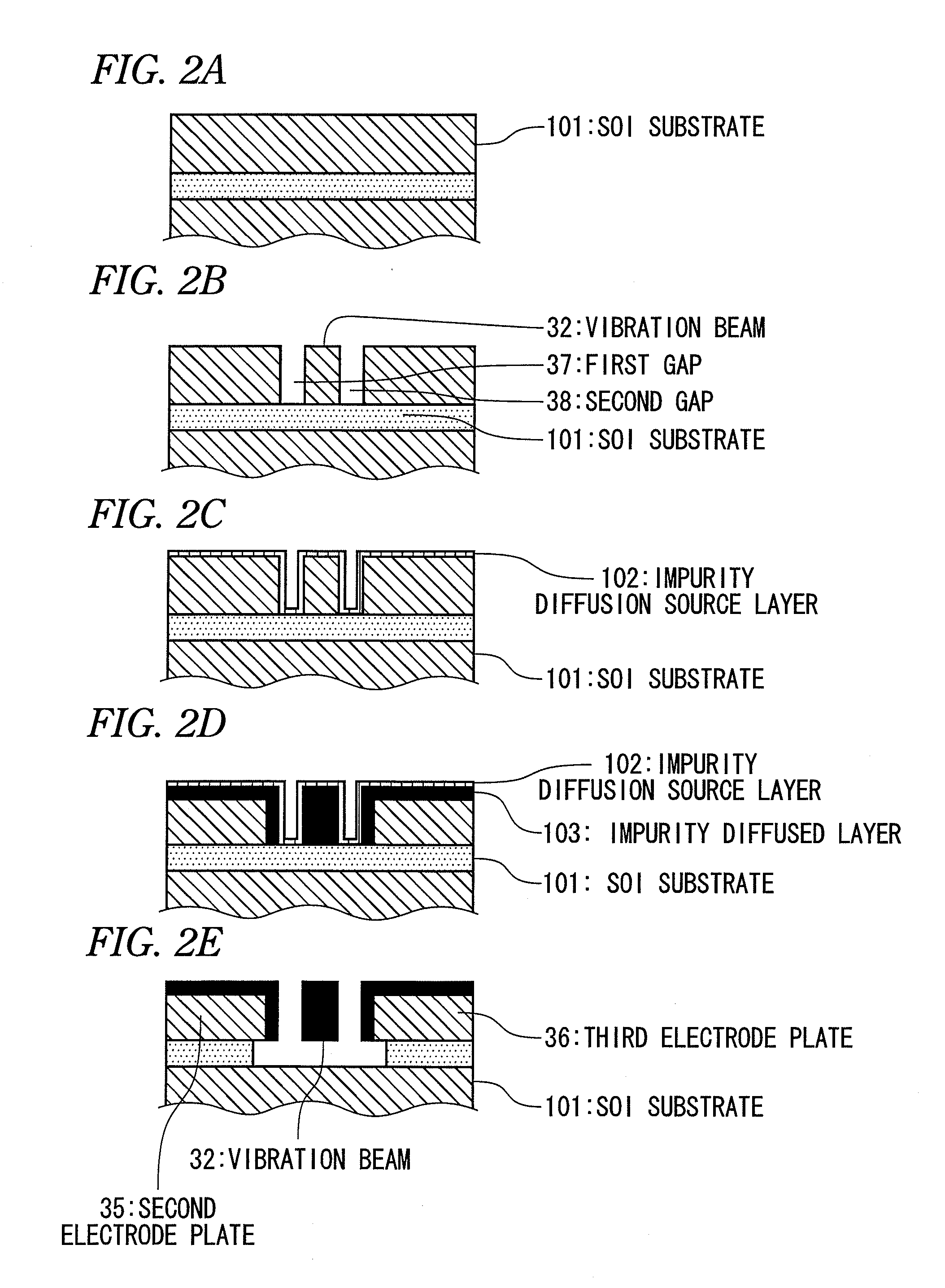
[0060]Hereinafter, exemplary embodiments of the present invention will be described with reference to the accompanying drawings. In all the drawings for the explanation of the embodiments, the members having the same functions are represented by the same reference numerals, and repeated description thereof will be omitted.

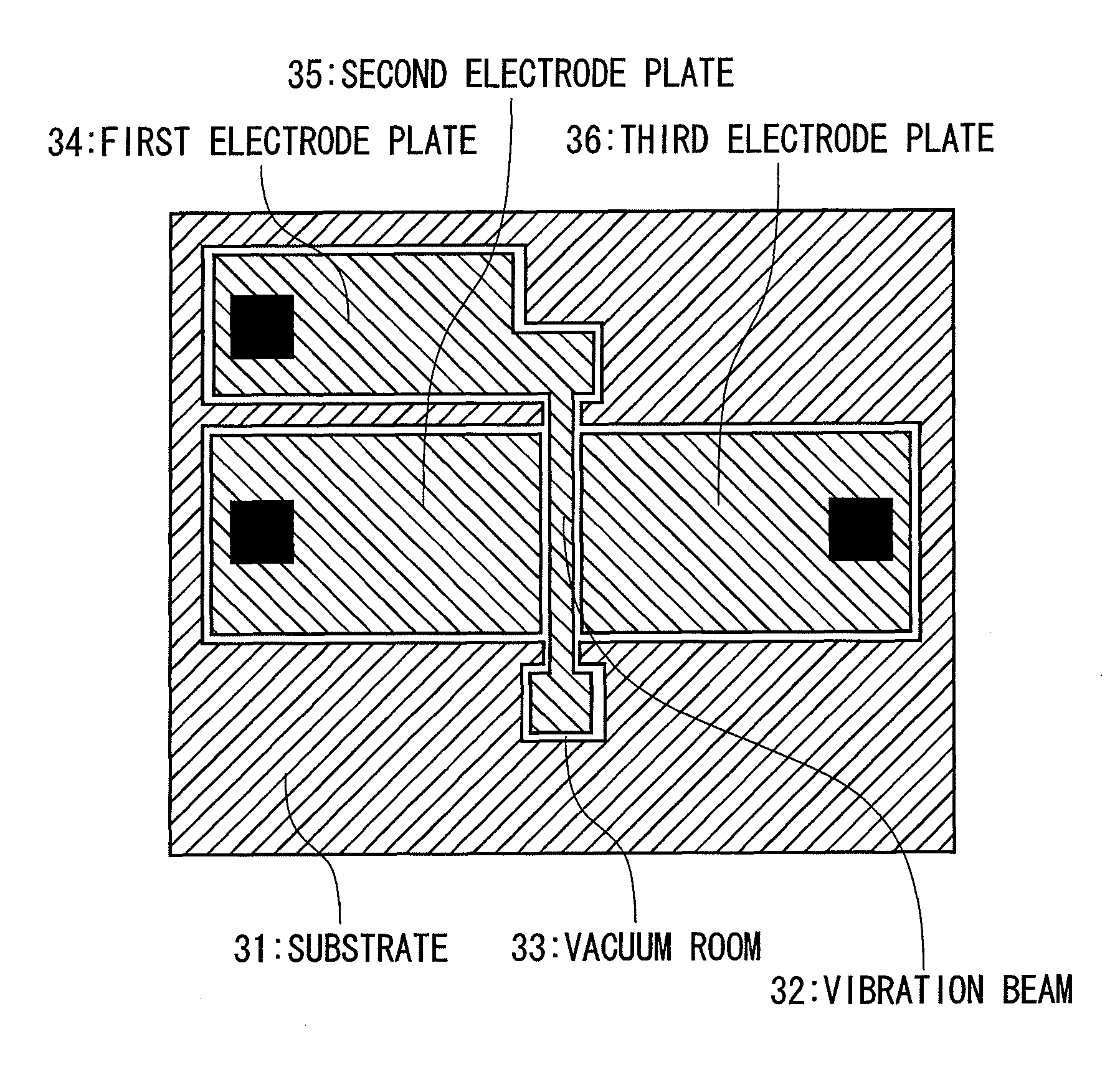
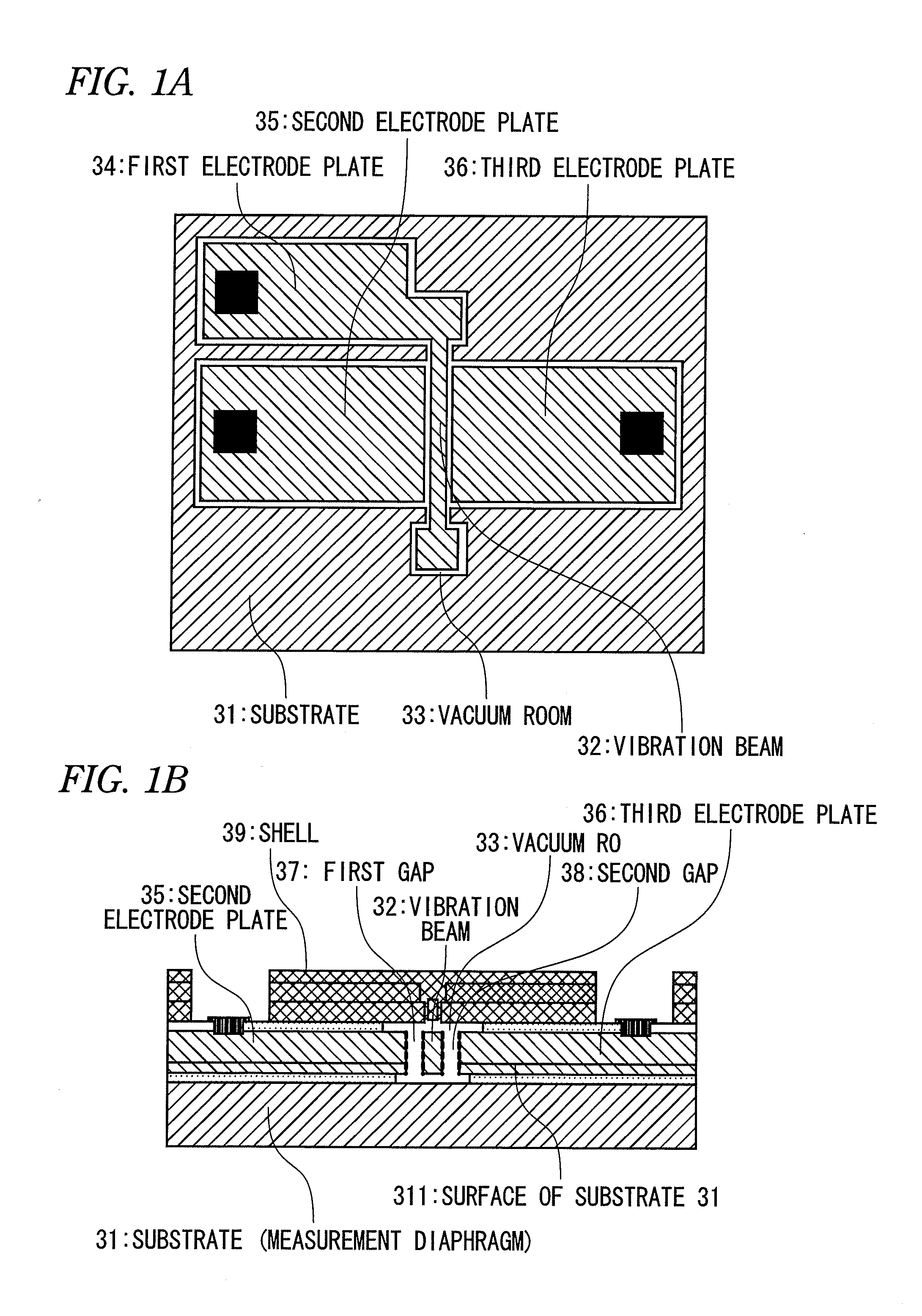
[0061]FIGS. 1A and 1B are a plan view and a sectional view, respectively, illustrating the structure of an essential part of an example resonant transducer manufactured by a manufacturing method according to the invention. The same views as FIGS. 1A and 1B are disclosed in US2012 / 0060607 A1, published on Mar. 15, 2012 and filed on Sep. 9, 2011 by the present Applicant Yokogawa Electric Corporation.

[0062]Referring to FIGS. 1A and 1B, a vibration beam 32 is a silicon single crystal disposed in a vacuum room 33 and is longer in the direction perpendicular to a surface 311 of a substrate 31 (measurement diaphragm) than in the direction parallel with the surface 311 in ...


PUM

PropertyMeasurementUnit
voltageaaaaaaaaaa
covalent bond radii Riaaaaaaaaaa

Abstract

A method of manufacturing a resonant transducer having a vibration beam includes: (a) providing an SOI substrate including: a first silicon layer; a silicon oxide layer on the first silicon layer; and a second silicon layer on the silicon oxide layer; (b) forming a first gap and second gap through the second silicon layer by etching the second silicon layer using the silicon oxide layer as an etching stop layer; (c) forming an impurity diffusion source layer on the second silicon layer; (d) forming an impurity diffused layer in a surface portion of the second silicon layer; (e) removing the impurity diffusion source layer through etching; and (f) removing at least a portion of the silicon oxide layer through etching such that an air gap is formed between the first silicon layer and a region of the second silicon layer surrounded by the first and second gaps.

Description

[0001]This application claims priority from Japanese Patent Applications No. 2011-264543, filed on Dec. 2, 2011, the entire contents of which are herein incorporated by reference.BACKGROUND[0002]1. Technical Field[0003]Embodiments described herein relate to a method of manufacturing a resonant transducer.[0004]2. Related Art[0005]FIGS. 6-17 illustrate the configuration of an essential part of a related-art resonant transducer. FIG. 6 illustrates the structure of an essential assembly, FIGS. 7-15 illustrate a manufacturing process, FIGS. 16A and 16B illustrate a circuit corresponding to the essential assembly of FIG. 6, and FIG. 17 illustrates the operation of the related-art resonant transducer.[0006]A manufacturing process will be described below. As shown in FIG. 7, a silicon oxide film 10a is formed on an n-type silicon single crystal substrate 1 and then patterned. A recess is formed in the substrate 1 by undercutting it in an oxide-film removed region, and p+ single crystal sil...

Claims


Application Information

Patent Timeline
Patent Type & Authority Applications(United States)
IPC IPC(8): H04R31/00
CPCH04R31/00B81C2201/0173B81C1/0015Y10T29/49005B81C1/00666H03H3/0072B81B2201/0271B81C2201/0164
Inventor NODA, RYUICHIROYOSHIDA, TAKASHI
Owner YOKOGAWA ELECTRIC CORP
Why Eureka
Try Eureka