

Through Silicon Via and Method of Manufacturing the Same
a technology of through silicon and manufacturing method, which is applied in the direction of semiconductor devices, semiconductor/solid-state device details, electrical devices, etc., can solve the problems of difficult failure of devices, and difficulty in conventional ecp processes to achieve uniform plating surface, etc., to avoid loading effect, improve tsv structure and manufacturing method, and improve the effect of filling uniformity
- Summary
- Abstract
- Description
- Claims
- Application Information
AI Technical Summary
Benefits of technology
Problems solved by technology
Method used
Image

Examples
Embodiment Construction
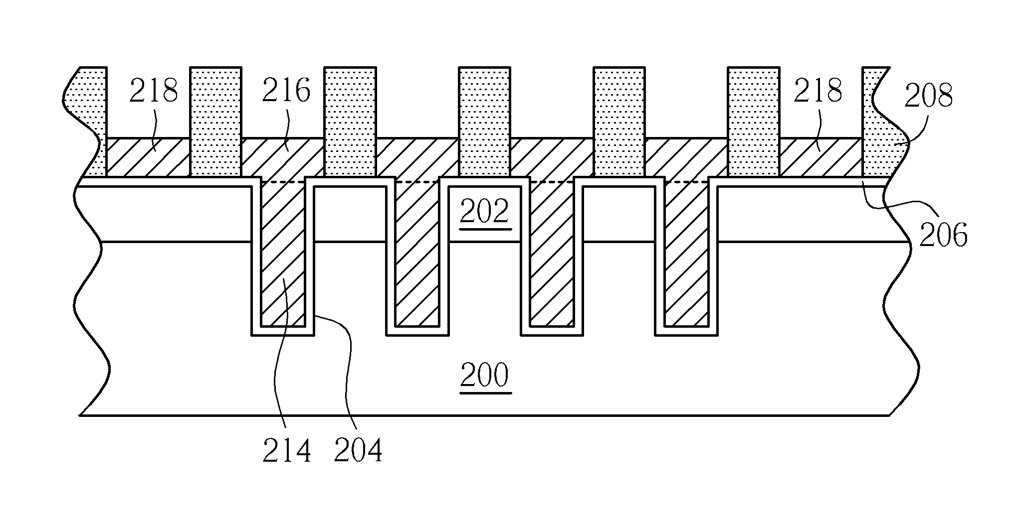
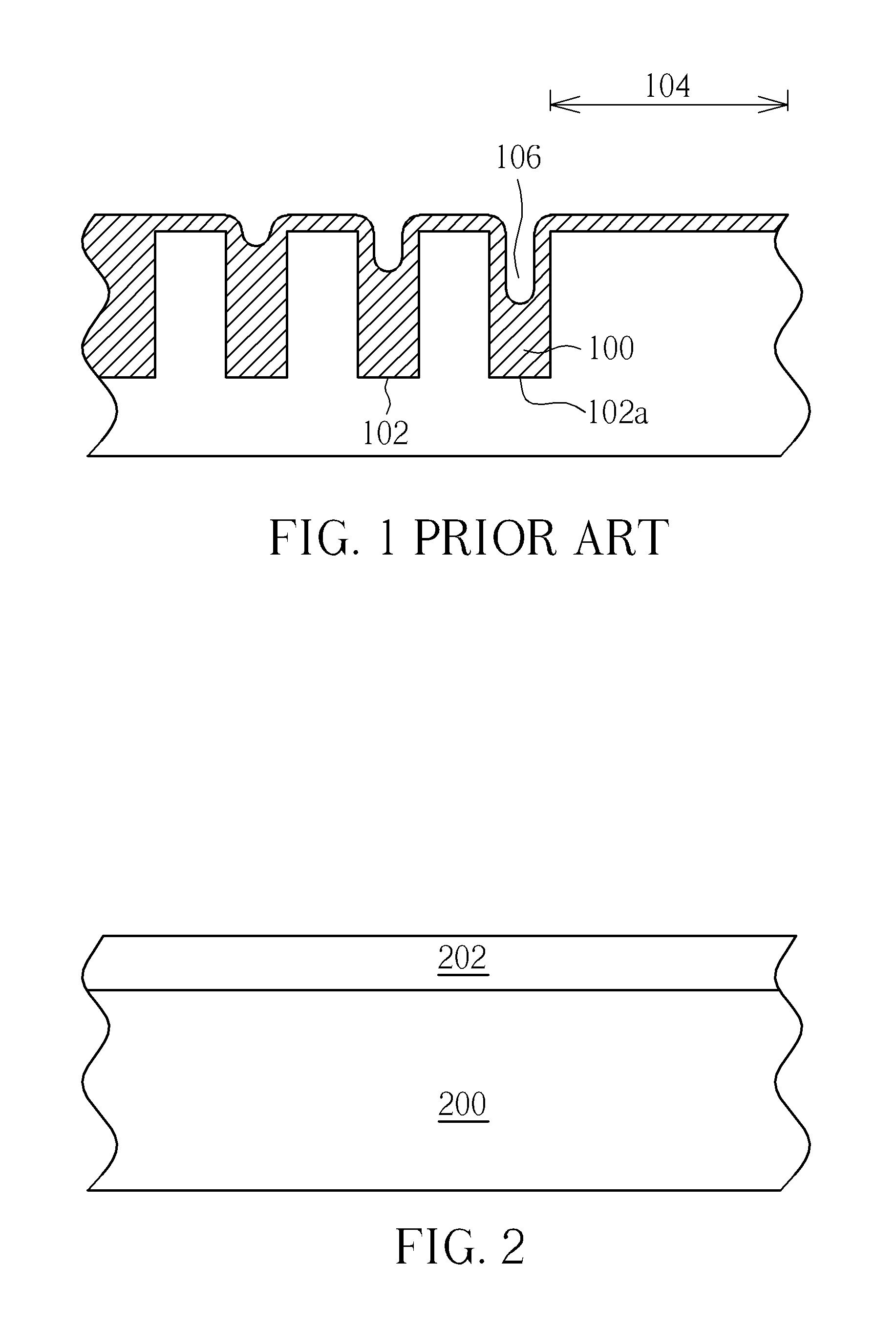
[0019]Please refer to FIGS. 2-8. FIGS. 2-8 show sequential cross-sectional views of the process flow in accordance to the present invention. First, as shown in FIG. 2, a substrate 200 is provided. The material of the substrate 200 may be monocrystalline silicon, gallium arsenide (GaAs) or other well-known semiconductor material. In one embodiment of present invention, in via middle process for example, a FEOL process may be performed first on the surface of the substrate 200. For example, a standard metal-oxide semiconductor (MOS) transistor fabrication process is performed to form at least one MOS transistor (not shown), or another semiconductor device, on the semiconductor substrate 200. The MOS transistor could be a PMOS transistor, a NMOS transistor, or a CMOS transistor and the MOS transistor could also include typical transistor structures, including gates, spacers, lightly doped drains, source / drain regions and / or salicides. The detailed description is omitted herein.
[0020]Af...
PUM
 Abstract
Description
Claims
Application Information