Non-volatile memory device and method for fabricating the same

a non-volatile memory and memory device technology, applied in the direction of semiconductor devices, basic electric elements, electrical appliances, etc., can solve the problems of reducing the size of the non-volatile memory device, affecting the operation characteristics of the erase operation characteristics of the charge-trapping-type non-volatile memory device, and affecting the effect of the erase operation characteristics

Inactive Publication Date: 2013-06-27
SK HYNIX INC
View PDF5 Cites 183 Cited by
  • Summary
  • Abstract
  • Description
  • Claims
  • Application Information

AI Technical Summary

Benefits of technology

[0009]An embodiment of the present invention is directed to a non-volatile memory device that may improve erase operation characteristics by suppressing back tunneling of electr...

Problems solved by technology

However, erase operation characteristics of a charge-trapping-type non-volatile memory device are deteriorated due to back tunneling that occurs as the electrons are introduced to the charge storage layer through the charge blocking laye...

Method used


Image

  • Non-volatile memory device and method for fabricating the same
  • Non-volatile memory device and method for fabricating the same
  • Non-volatile memory device and method for fabricating the same

Examples


first embodiment

[0036]The non-volatile memory device in accordance with the present invention may be fabricated through the fabrication method described above.

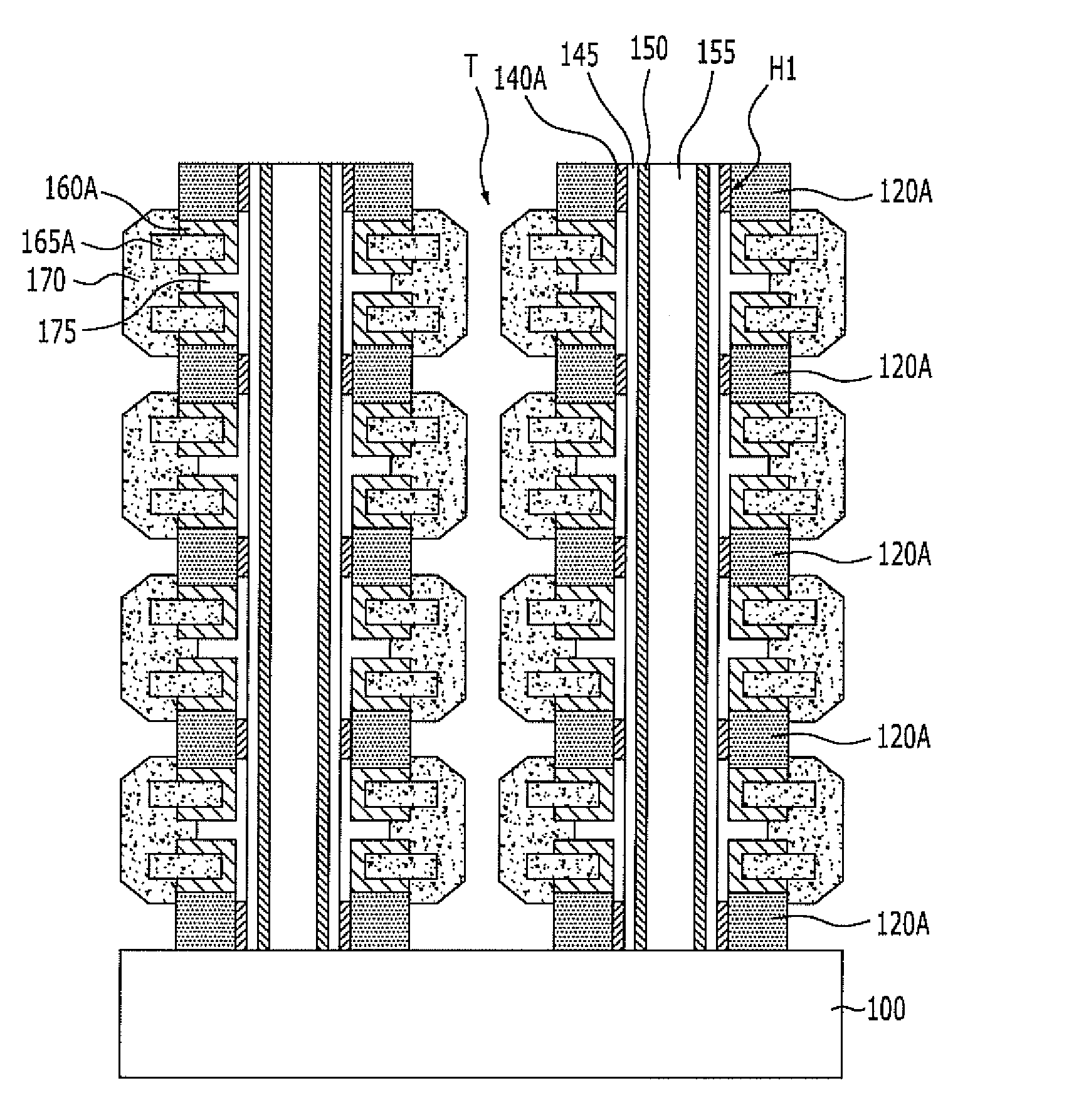
[0037]Referring to FIG. 1G, the non-volatile memory device in accordance with the first embodiment of the present invention includes the channel layer 155 that is extends vertically from the substrate 100, the multiple inter-layer dielectric layer patterns 120A and the multiple gate electrodes that are alternately stacked along the channel layer 155, the charge storage layer 145 interposed between the channel layer 155 and each gate electrode, the air gap 175 interposed between the gate electrode and the charge storage layer 145, the tunnel insulation layer 150 interposed between the charge storage layer 145 and the channel layer 155, and the barrier metal layer pattern 160A interposed between the inter-layer dielectric layer pattern 120A and the gate electrode.

[0038]Each of the gate electrodes may be formed of the first gate electrode layer ...

second embodiment

[0060]In the present invention, a pass gate electrode that includes the first pass gate electrode layer 105 and the second pass gate electrode layer 115 is formed in the lower portion of the gate structure, and the pass gate electrode includes a sub-channel layer for coupling a pair of main channel layers with each other.

[0061]According to an embodiment of the present invention, erase operation characteristics may be improved by suppressing back tunneling of electrons by substituting a charge blocking layer interposed between a gate electrode and a charge storage layer with an air gap, and a method for fabricating the non-volatile memory device.


PUM


Abstract

A non-volatile memory device includes a channel layer vertically extending from a substrate, a plurality of inter-layer dielectric layers and a plurality of gate electrodes that are alternately stacked along the channel layer, and an air gap interposed between the channel layer and each of the plurality of gate electrodes. The non-volatile memory device may improve erase operation characteristics by suppressing back tunneling of electrons by substituting a charge blocking layer interposed between a gate electrode and a charge storage layer with an air gap, and a method for fabricating the non-volatile memory device.

Description

CROSS-REFERENCE TO RELATED APPLICATIONS[0001]The present application claims priority of Korean Patent Application No. 10-2011-0140533, filed on Dec. 22, 2011, which is incorporated herein by reference in its entirety.BACKGROUND[0002]1. Field[0003]Exemplary embodiments of the present invention relate to a non-volatile memory device and a fabrication method thereof, and more particularly, to a non-volatile memory device having a three-dimensional structure where a plurality of memory cells are stacked vertically from a substrate, and a method for fabricating the non-volatile memory device.[0004]2. Description of the Related Art[0005]Non-volatile memory devices retain data although power is turned off. Currently, various nonvolatile memory devices, such as a flash memory, have been widely used.[0006]As the integration degree of a non-volatile memory device having a two-dimensional structure where memory cells are formed in a single layer may reach a limit, a non-volatile memory device ...

Claims


Application Information

Patent Timeline
IPC IPC(8): H01L29/792H01L21/20
CPCH01L27/11582H01L29/792H01L29/40117H10B43/27H01L21/76205H01L21/7682H01L29/66833H01L29/66666
Inventor KIM, MIN-SOOSHEEN, DONG-SUNPYI, SEUNG-HOWHANG, SUNG-JIN
Owner SK HYNIX INC
Why Eureka
Try Eureka