

High resistivity silicon-on-insulator substrate and method of forming
- Summary
- Abstract
- Description
- Claims
- Application Information
AI Technical Summary
Benefits of technology
Problems solved by technology
Method used
Image

Examples
Embodiment Construction
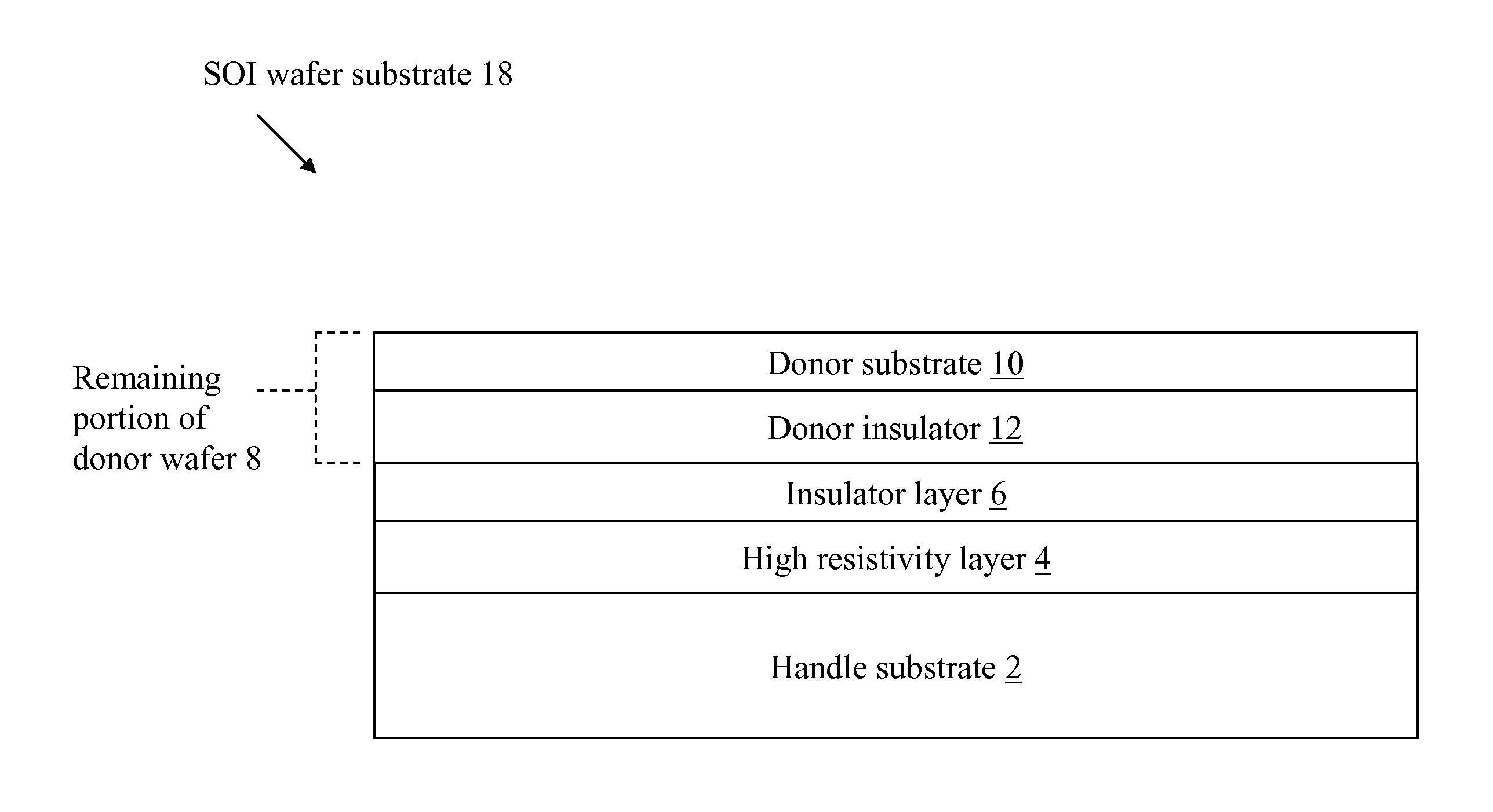
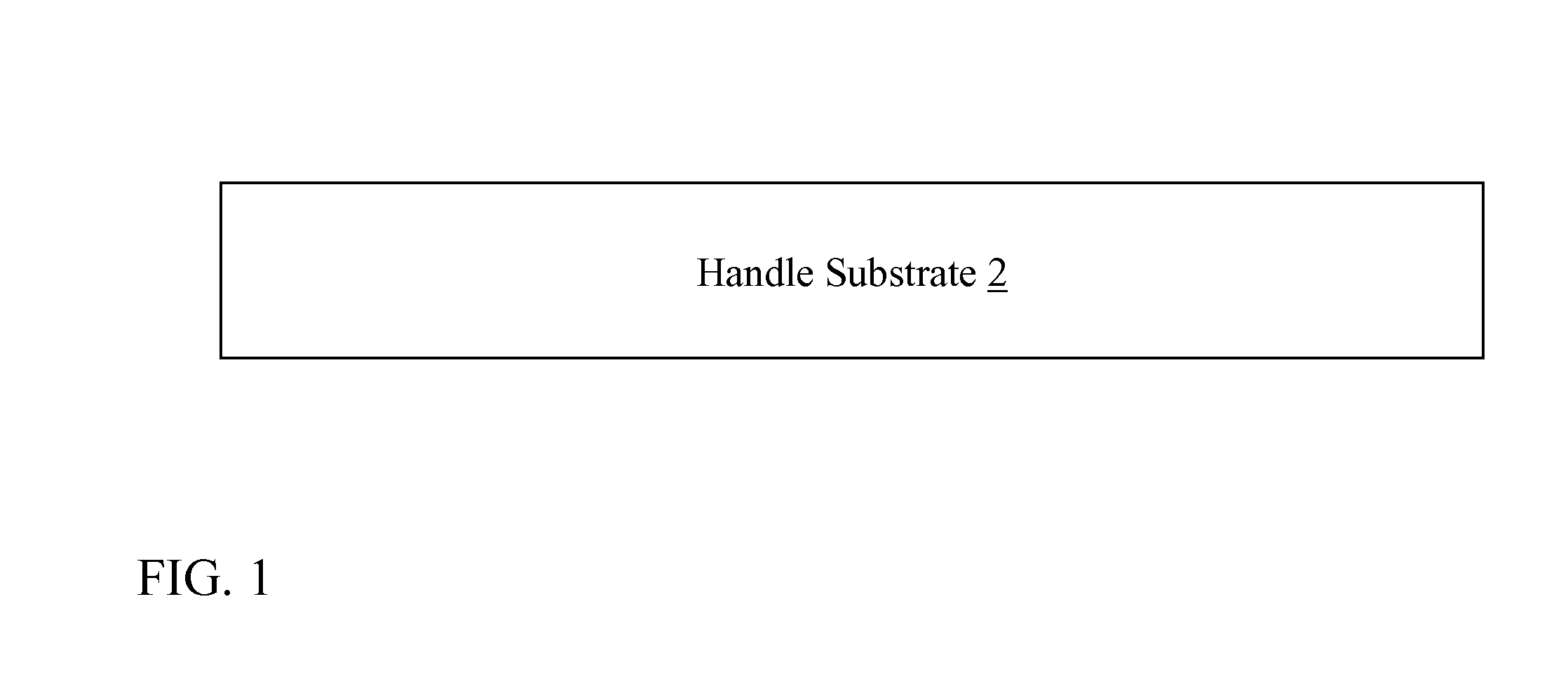
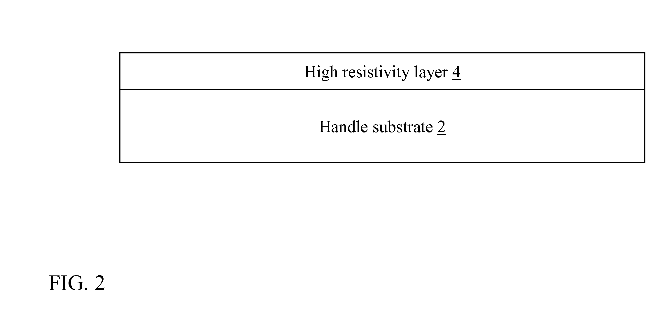
[0015]As noted herein, the subject matter disclosed relates to a silicon-on-insulator based integrated circuit structure. More specifically, the subject matter disclosed herein relates to an integrated circuit structure having a silicon-on-insulator substrate with a high resistivity.
[0016]In certain semiconductor devices, such as semiconductor-on-insulator (SOI) radio frequency (RF) devices, resistivity in the handle substrate can impact performance of the device. An example of such a device is a SOI RF complementary metal oxide semiconductor (CMOS) device. In these SOI RF devices, electric potentials on transistors and wires create electric fields, which in turn can cause movement of free carriers in the handle substrate. The movement of carriers is generally non-linear, and this non-linear “drag” both lowers the charge (Q) of passive components and creates nonlinearities in electrical characteristics. The handle substrate also acts as a path for heat removal from the active device...
PUM
 Abstract
Description
Claims
Application Information