Touch panel device and display device with touch panel device

a technology of touch panel and display device, which is applied in the field can solve the problems of difficult detachment of touch panel device, weight increase, and difficulty in filling

Active Publication Date: 2013-07-04
TEIJIN KASEK KK
View PDF25 Cites 23 Cited by
  • Summary
  • Abstract
  • Description
  • Claims
  • Application Information

AI Technical Summary

Benefits of technology

[0018]According to the touch panel device of the present invention, and the display device equipped with a touch panel device of the present invention...

Problems solved by technology

(1) Since a touch panel device and a display device differ in production conditions, it is difficult or impossible to integrally produce the touch panel device and the display device so as to completely eliminate any clearance. Further, when the touch panel device and the display device are not integrally produced, if it is found, at the final stage of production, that the touch panel device does not suitably work, it is possible to detach the touch panel device, which does not suitably work, from the display surface of the display device, and exchange it with a new touch panel device. Therefore, the touch panel device and the display device are preferably not integrally produced.
(2) If the thickness of the air layer between the touch panel device and the display device is too small, the light reflected at the interface between the touch panel device and the air layer (i.e., the top side interface of the air layer), and the light reflected at the interface between the display device and the air layer (i.e., the bottom side interface of the air layer) interfere with each other, and thereby Newton r...

Method used


Image

  • Touch panel device and display device with touch panel device
  • Touch panel device and display device with touch panel device
  • Touch panel device and display device with touch panel device

Examples


examples

[0067]The various measurements in the examples were performed as follows:

[0068]

[0069]For the linear expansion coefficient of the film, a 4 mm width×30 mm sample was left at a temperature of 25° C. and a relative humidity of 50% for 24 hours, then a thermal stress-strain measuring device (SII Nanotechnology SS6100) was used for measurement three times by a temperature elevation rate of 5° C. / min to calculate the linear expansion coefficient in the temperature range of 20° C. to 60° C. The average value was determined.

[0070]

[0071]A JASCO spectroellipsometer M220 was used to measure retardation with a light wavelength of 550 nm.

Reference Example

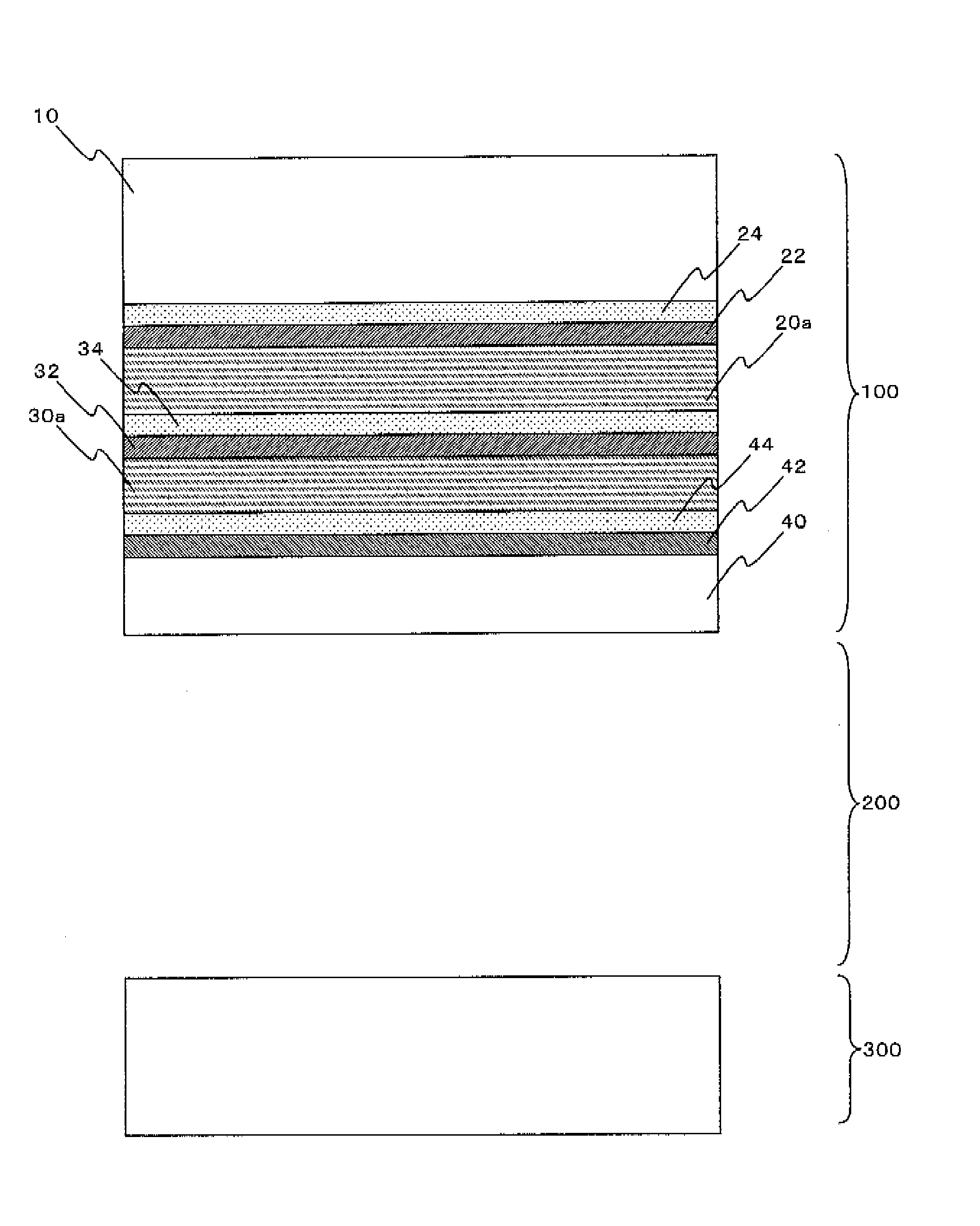
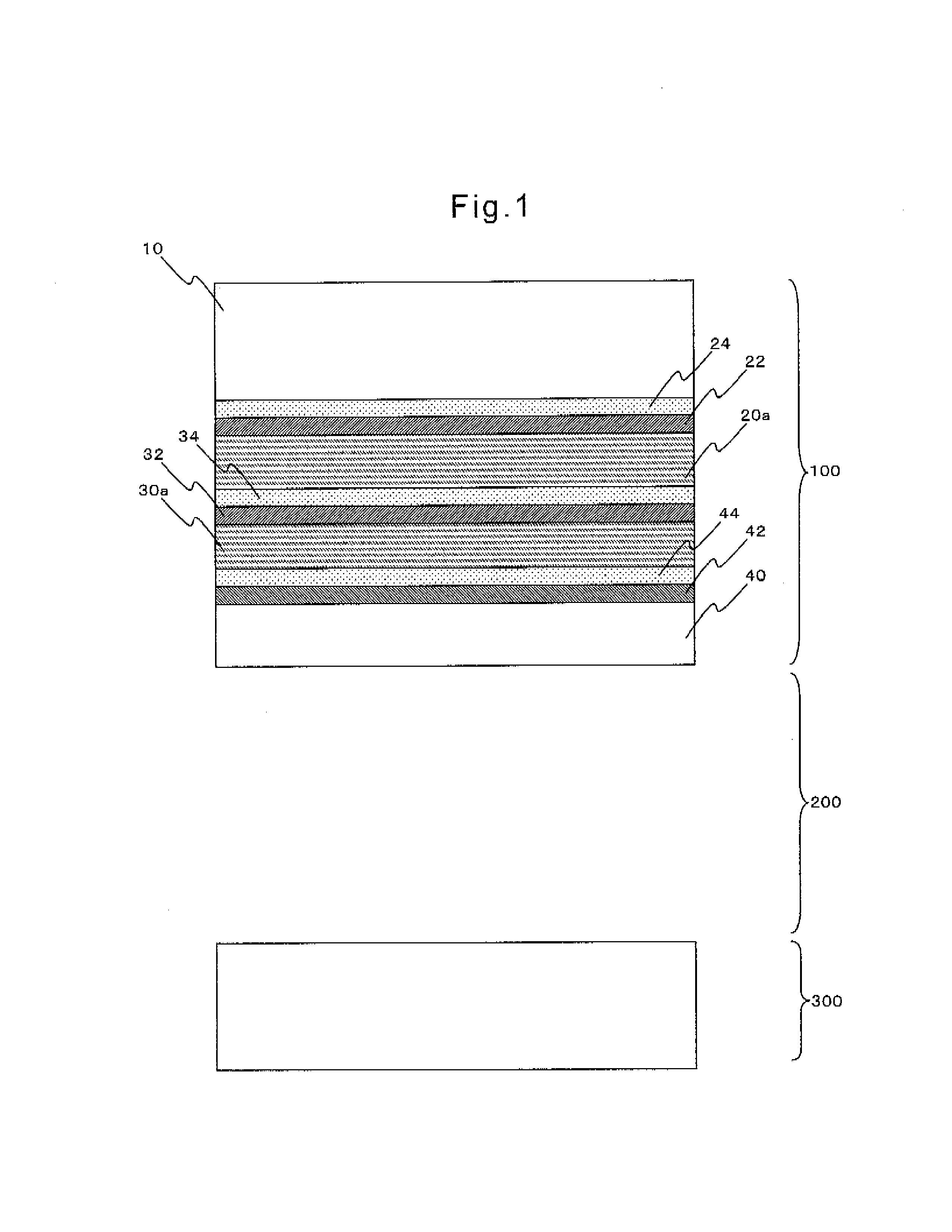
[0072]An electrostatic capacitance-type display device equipped with a touch panel device of a reference example was prepared to obtain the configuration as shown in FIG. 1. Specifically, the following procedure was performed to prepare the electrostatic capacitance-type display device equipped with a touch panel device of a reference example.

[0...

example 1

[0095]The electrostatic capacitance-type display device equipped with a touch panel device of Example 1 was prepared to obtain the configuration as shown in FIG. 3. Specifically, the following procedure was performed to prepare the electrostatic capacitance-type display device equipped with a touch panel device of Example 1.

[0096](1) Preparation of Electrostatic Capacitance-Type Display Device Equipped with Touch Panel Device

[0097]Except for using first and second polymer films having position-detecting electrode layers (20b, 22; 30b, 32) and made of unstretched polycarbonate (PC) films (20b, 30b), instead of first and second polymer films having position-detecting electrode layers (20a, 22; 30a, 32) and made of biaxially stretched polyethylene terephthalate (PET) films (20a, 30a), the same procedure was repeated as the comparative example to prepare an electrostatic capacitance-type display device equipped with a touch panel device of Example 1.

[0098]The thus obtained electrostatic...

example 2

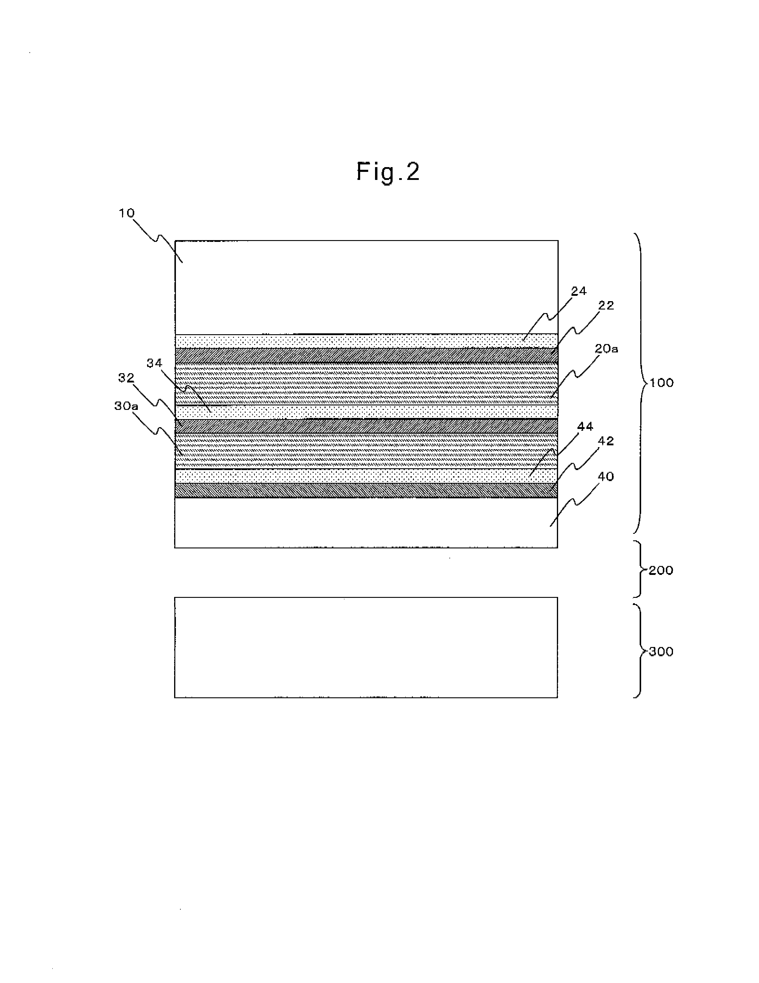
[0104]The electrostatic capacitance-type display device equipped with a touch panel device of Example 2 was prepared to obtain the configuration as shown in FIG. 4. Specifically, the following procedure was performed to prepare the electrostatic capacitance-type display device equipped with a touch panel device of Example 2.

[0105](1) Preparation of Electrostatic Capacitance-Type Display Device Equipped with Touch Panel Device

[0106]The same procedure was repeated as Example 1 to prepare an electrostatic capacitance-type display device equipped with a touch panel device of Example 2, excepting the followings: a 100 μm-thick polarizing film was bonded, through an adhesive comprised of acrylic resin, between a protective transparent substrate of 0.5 mm-thick Corning super-hard glass and a first polymer film having a position-detecting electrode layer (20a, 22); a first polymer film (20c, 22) having a position-detecting electrode layer and made of a monoaxially stretched polycarbonate (P...


PUM


Abstract

Provided is a touch panel device which prevents a problem such as generation of Newton's rings even if an air layer between the touch panel device and a display device has a small thickness. This capacitance type touch panel device (100) includes: a protective transparent base (10) having an observation-side surface and a display device-side surface; and two polymer films with position detection electrode layers (20b, 22; 30b, 32) which are arranged on the display device-side surface of the protective transparent base. The difference between the minimum value and the maximum value of the linear expansion coefficients in the surface direction of all the polymer films (20b; 30b) arranged on the display device-side surface of the protective transparent base is 10.0×10⁻⁶ cm/cm. ° C. or below. Furthermore, the display device with a touch panel device (100, 200, 300) according to the present invention has such a touch panel device.

Description

TECHNICAL FIELD[0001]The present invention relates to a touch panel device, and more particularly an electrostatic capacitance-type touch panel device. Further, the present invention relates to a display device equipped with a touch panel device.BACKGROUND ART[0002]Display devices equipped with touch panel devices, e.g. liquid crystal displays equipped with touch panel devices, are used for mobile phones and other mobile electronic devices, consumer electronics, and unmanned reception devices and other stationary-type customer assistance terminals.[0003]As touch panel devices, contact film types, electrostatic capacity types, photosensor types, etc. are known. Among these, electrostatic capacitance-type touch panel devices are excellent in transmission rate of light from the display devices, durability, etc. Further, electrostatic capacitance-type touch panel devices are excellent in the point that they enable multipoint detection (multi-touch) by arranging, as a vertical and horizo...

Claims


Application Information

Patent Timeline
IPC IPC(8): G06F3/044
CPCG06F3/0412G02F1/13338G06F3/044G06F3/0445G06F2203/04103
Inventor IMAMURA, KOICHIITO, HARUHIKOIKEDA, KOKI
Owner TEIJIN KASEK KK
Why Eureka
Try Eureka