
Optical device structures with the light outcoupling layers

a technology of optical devices and light outcoupling layers, which is applied in the direction of light and heating equipment, transportation and packaging, synthetic resin layered products, etc., can solve the problems of 20% of light to be emitted from the front of the device, and the inability of fabricated ito films to sinter (annealing) at a high temperature, so as to reduce the surface resistance value and refraction index of the upper conductive films. , the effect of efficient improvement of ligh

Active Publication Date: 2013-07-04
IND TECH RES INST
View PDF1 Cites 9 Cited by
  • Summary
  • Abstract
  • Description
  • Claims
  • Application Information

AI Technical Summary

Benefits of technology

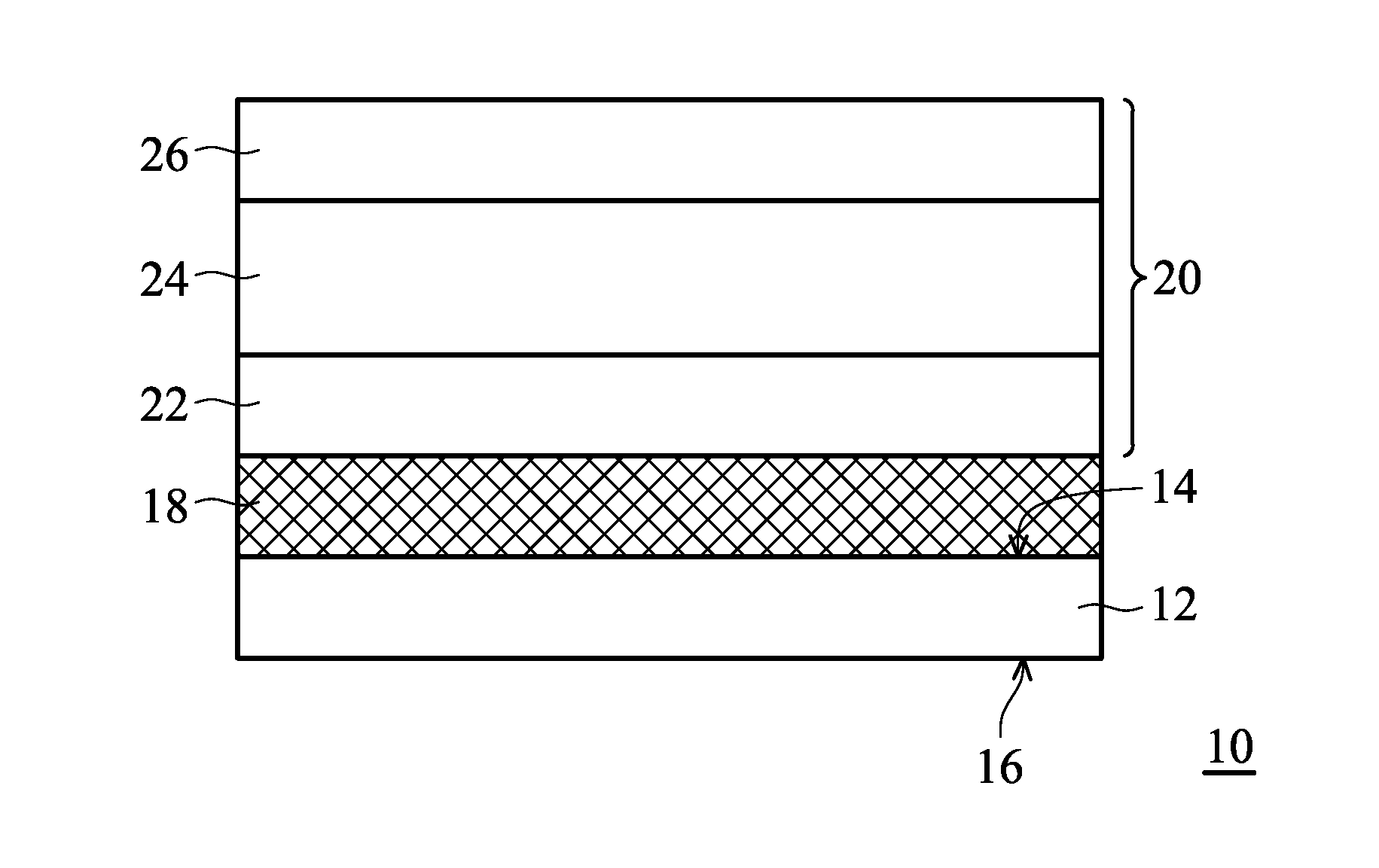
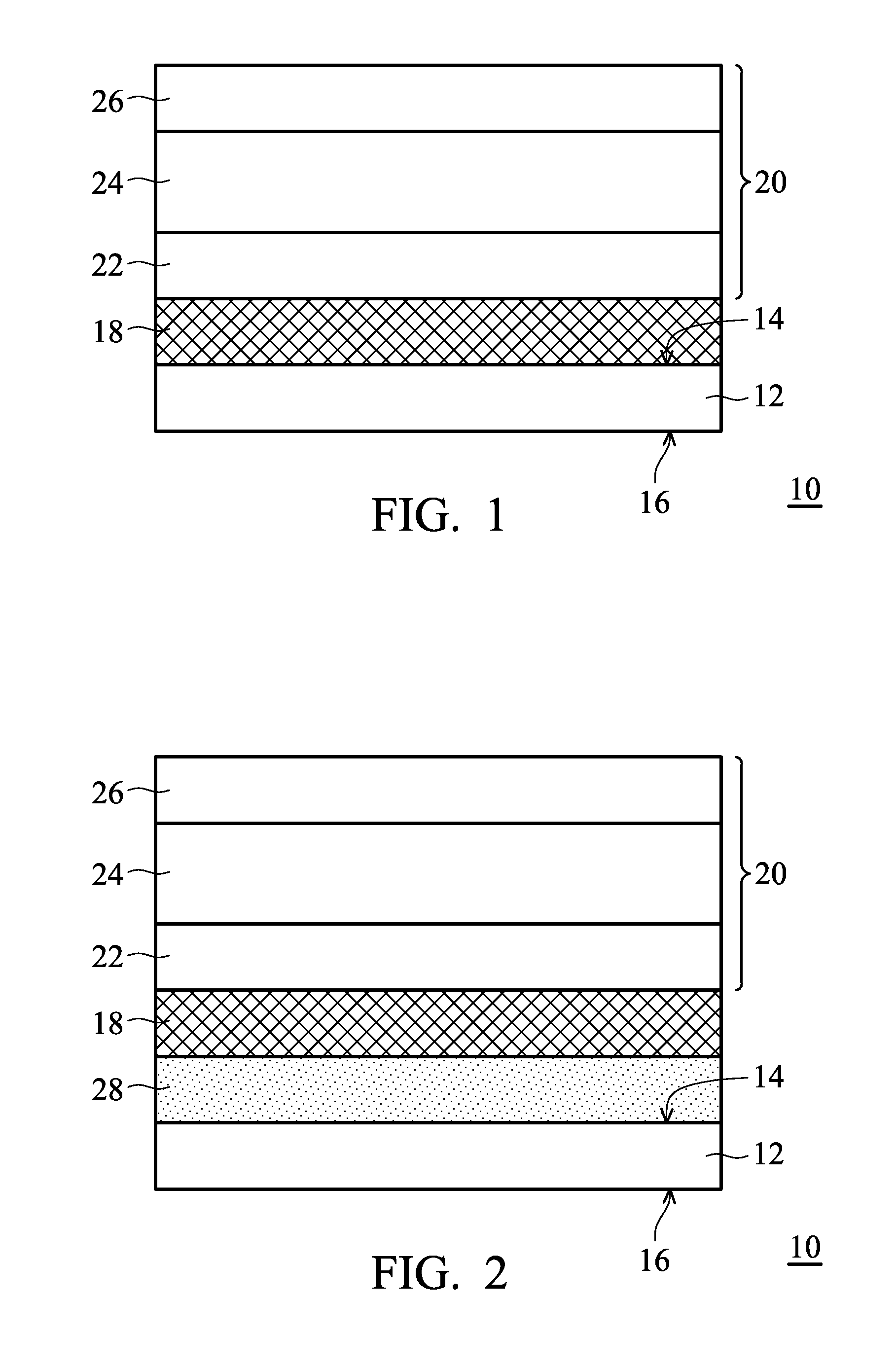
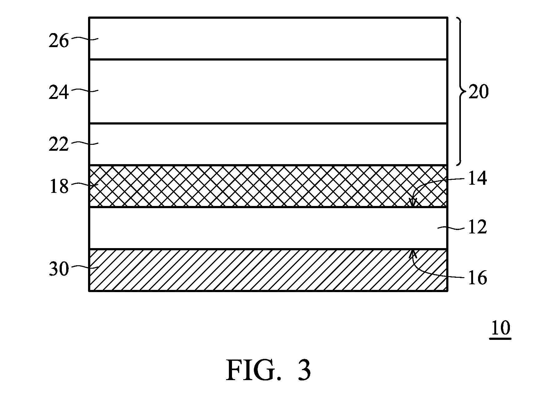
The patent provides an optical device structure that improves the efficiency of light outcoupling in OLED devices. It uses a polyimide material as a light outcoupling layer with high heat resistance and a refraction index close to that of the OLED components. After annealing, the surface resistance of the upper conductive film is decreased, and the penetration rate improved, resulting in higher luminous efficiency. Combining an outer microlens with the OLED further improves efficiency. The polyimide material also planarizes the surface of the thin film formed by particles, which can improve device lifespan. This light outcoupling structure increases light outcoupling efficiency and can be used in OLED devices.

Problems solved by technology

However, the distinction of the refraction index between various layers in an OLED is large (mismatch of refraction index) which causes only 20% of light to be emitted from the front of the device.
If the materials which cannot endure high temperature are used as the light outcoupling layer, the fabricated ITO film is incapable of sintering (annealing) at a high temperature.

Method used


Image

  • Optical device structures with the light outcoupling layers
  • Optical device structures with the light outcoupling layers
  • Optical device structures with the light outcoupling layers

Examples


example 1

Preparation and Physical Properties of the Polyimide (PI-1)

[0025]A polyimide comprising 2,2-bis[4-(4-aminophenoxy)phenyl]propane A and bicyclo[2,2,2]oct-7-ene-2,3,5,6-tetracarboxylic dianhydride B with a composition ratio of 5:5 was prepared. First, 82.7 g of 2,2-bis[4-(4-aminophenoxy)phenyl]propane A, 50 g of bicyclo[2,2,2]oct-7-ene-2,3,5,6-tetracarboxylic dianhydride B and 530.8 g of m-cresol were added to a 2 L glass reactor and reacted with electric stirring under 220° C. for 4 hours to form a polyimide solution with a solid content of 20%. The polyimide solution was then re-precipitated with methanol. After drying, filamentous polyimide (PI) was obtained. The filamentous polyimide (PI) was dissolved by dimethyl acetamide to prepare a polyimide (PI-1) solution with a solid content of 15%.

[0026]In this example, the b value (yellow value) of the prepared polyimide (PI-1) was 2.37.

example 2

Preparation and Physical Properties of the Polyimide (PI-2)

[0027]A polyimide comprising 2,2-bis[4-(4-aminophenoxy)phenyl]propane A, 4,4-diaminodiphenyl ether B and pyromellitic dianhydride C with a composition ratio of 3:7:10 was prepared. First, 28.2 g of 2,2-bis[4-(4-aminophenoxy)phenyl]propane A, 32.1 g of 4,4-diaminodiphenyl ether B, 50 g of pyromellitic dianhydride C and 441.4 g of m-cresol were added to a 2 L glass reactor and reacted with electric stirring under 220° C. for 4 hours to form a polyimide solution with a solid content of 20%. The polyimide solution was then re-precipitated with methanol. After drying, filamentous polyimide (PI) was obtained. The filamentous polyimide (PI) was dissolved by dimethyl acetamide to prepare a polyimide (PI-2) solution with a solid content of 15%.

[0028]In this example, the b value (yellow value) of the prepared polyimide (PI-2) was 1.95.

example 3

Preparation and Physical Properties of the Polyimide (PI-3)

[0029]A polyimide comprising 2,2-bis[4-(4-aminophenoxy)phenyl]propane A and bicyclo[2,2,2]oct-7-ene-2,3,5,6-tetracarboxylic dianhydride B with a composition ratio of 5:5 was prepared. First, 82.7 g of 2,2-bis[4-(4-aminophenoxy)phenyl]propane A, 50 g of bicyclo[2,2,2]oct-7-ene-2,3,5,6-tetracarboxylic dianhydride B and 530.8 g of m-cresol were added to a 2 L glass reactor and reacted with electric stirring under 220° C. for 4 hours to form a polyimide solution with a solid content of 20%. The polyimide solution was then re-precipitated with methanol. After drying, filamentous polyimide (PI) was obtained. The filamentous polyimide (PI) was dissolved by dimethyl acetamide to prepare a polyimide (PI-3) solution with a solid content of 15%.

[0030]In this example, the b value (yellow value) of the prepared polyimide (PI-3) was 2.37.


PUM

PropertyMeasurementUnit
Thicknessaaaaaaaaaa

Abstract

An optical device structure with a light outcoupling layer is provided. The optical device structure includes a substrate having a first surface and a second surface, and a layer of polyimide (PI) or its copolymer formed on the first surface of the substrate, wherein the layer of polyimide or its copolymer is prepared from at least one aromatic diamine and at least one cycloaliphatic dianhydride, and an optical component formed on the layer of polyimide or its copolymer.

Description

CROSS REFERENCE TO RELATED APPLICATIONS[0001]This application claims priority of Taiwan Patent Application No. 100149461, filed on Dec. 29, 2011, the entirety of which is incorporated by reference herein.BACKGROUND[0002]1. Technical Field[0003]The technical field relates to an optical device structure comprising a layer of polyimide (PI) or its copolymer.[0004]2. Description of the Related Art[0005]Organic light emitting diodes (OLEDs) have been deemed as a rising star of flat panel displays or the lighting industry due to superior characteristics thereof including light weight, thin profile, self-luminescence, low power consumption, no requirement of a backlight source, no limitation of viewing angle and rapid response time etc. In order to be more competitive in the display and lighting markets, R & D units in the world invest a great deal of funds and human resources to improve device efficiency. In addition to the development of interior luminescent materials, exterior light out...

Claims


Application Information

Patent Timeline
IPC IPC(8): B32B17/10H01L51/54F21V5/04B32B27/14B32B5/02
CPCH01L51/0077H01L51/0081Y10T428/269H01L51/5262H01L51/5275H01L51/0085Y10T428/31721Y10T428/31623H10K85/30H10K85/324H10K85/342H10K59/879H10K50/85H10K50/858
Inventor HUANG, YUEH-CHUANLEU, CHYI-MINGHSIEH, MENG-TING
Owner IND TECH RES INST
Learn More