Transmissive image modulator including stacked diode structure having multi absorption modes

a transmissive image and modulator technology, applied in the field of transmissive image modulators, can solve the problems of high voltage, high cost, and inability to accurately obtain distance information, and achieve the effect of low driving voltage and high transmissivity differen

Active Publication Date: 2013-07-11
SAMSUNG ELECTRONICS CO LTD +1
View PDF10 Cites 25 Cited by
  • Summary
  • Abstract
  • Description
  • Claims
  • Application Information

AI Technical Summary

Benefits of technology

[0013]One or more exemplary embodiments may provide transmissive light modulators which are capable of modulating images across a wide bandwidth, operate with relatively low driving voltages, and have high transmissivity difference.

Problems solved by technology

However, using the above-stated methods, the accuracy of distance information rapidly deteriorates as a distance to an object increases.
Furthermore, the above methods depend on surface condition of the object, and thus, it is difficult to acquire precise distance information.
However, such light modulators feature large volumes, use high voltage of several kV, and are expensive.
However, there is a trade-off between an ON / OFF reflectivity difference and bandwidth, and thus, it is difficult to increase ON / OFF reflectivity difference and bandwidth simultaneously.
Meanwhile, since a reflective light modulator reflects modulated light, a light path for providing the modulated light to an imaging device (CCD or CMOS) is complicated, and thus, it is necessary to configure an additional optic system.
If an driving voltage of a light modulator increases, power consumption increases in proportion to the square of the driving voltage.
Increased power consumption causes increased heat generated by an image modulator, and thus, the performance of the image modulator may deteriorate due to the generated heat.

Method used


Image

  • Transmissive image modulator including stacked diode structure having multi absorption modes
  • Transmissive image modulator including stacked diode structure having multi absorption modes
  • Transmissive image modulator including stacked diode structure having multi absorption modes

Examples


Embodiment Construction

[0068]Reference will now be made in detail to exemplary embodiments which are illustrated in the accompanying drawings, wherein like reference numerals refer to the like elements throughout. In this regard, the present embodiments may have different forms and should not be construed as being limited to the descriptions set forth herein. Accordingly, exemplary embodiments are merely described below, by referring to the figures, to explain aspects of the present description.

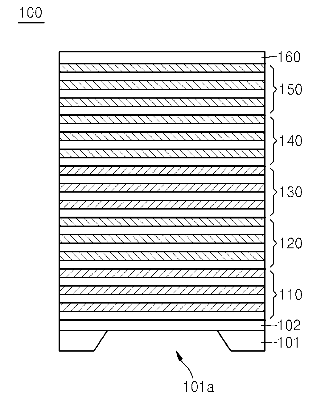
[0069]FIG. 1 is a schematic sectional view showing a stacked structure of a transmissive light modulator 100 according to an exemplary embodiment. Referring to FIG. 1, the transmissive light modulator 100 according to the present embodiment may include a substrate 101, a first contact layer 102 arranged on the substrate 101, a first distributed Bragg reflector (DBR) layer 110 arranged on the first contact layer 102, a first active layer 120 which has a multiquantum well (MQW) structure and is arranged on the first ...


PUM


Abstract

A transmissive light modulator including a first reflection layer; a first active layer, arranged on the first reflection layer and including a plurality of quantum well layers and a plurality of barrier layers; a second reflection layer arranged on the first active layer; a second active layer, arranged on the second reflection layer and including a plurality of quantum well layers and a plurality of barrier layers; and a third reflection layer arranged on the second active layer, wherein the first reflection layer and the third reflection layer are each doped with a first type dopant, and the second reflection layer is doped with a second type dopant, which is electrically opposite to the first type dopant.

Description

CROSS-REFERENCE TO RELATED APPLICATION[0001]This application claims priority from Korean Patent Application No. 10-2012-0001550, filed on Jan. 5, 2012, in the Korean Intellectual Property Office, the disclosure of which is incorporated herein in its entirety by reference.BACKGROUND[0002]1. Field[0003]Apparatuses and methods consistent with exemplary embodiments relate to transmissive image modulators, and more particularly, to transmissive image modulators capable of modulating images across a wide bandwidth by employing a stacked diode structure having multi absorption modes.[0004]2. Description of the Related Art[0005]An image captured by using a common camera does not include information regarding a distance between the camera and an object. To embody a 3-dimensional (3D) image capturing apparatus, such as a 3D camera, an additional device for measuring distances from a plurality of points on surfaces of an object is necessary. Distance information with respect to an object may b...

Claims


Application Information

Patent Timeline
Patent Type & Authority Applications(United States)
IPC IPC(8): H01L31/0352H01L31/18
CPCB82Y20/00G02F2203/12H01L31/035236G02F1/017A47J47/02B65D1/10A47J36/10A47J41/0088A47J36/04B65D43/00B65D2543/00296
Inventor CHO, YONG-CHULLEE, YONG-TAKYOU, JANG-WOONA, BYUNG-HOONPARK, YONG-HWAPARK, CHANG-YOUNGCHIO, HEE-JUJU, GUN-WU
Owner SAMSUNG ELECTRONICS CO LTD
Why Eureka
Try Eureka