Wiring board and method of manufacturing the same

a wiring board and manufacturing method technology, applied in the direction of manufacturing tools, soldering apparatus, semiconductor/solid-state device details, etc., can solve the problems of difficult to form high solder bumps, poor connection between respective pads and ic chips, and difficulty in forming high solder bumps. , the volume of the protruding member can increase, and the internal diameter of the opening portion decreases.

Inactive Publication Date: 2013-07-18
NGK SPARK PLUG CO LTD
View PDF19 Cites 37 Cited by
  • Summary
  • Abstract
  • Description
  • Claims
  • Application Information

AI Technical Summary

Benefits of technology

[0013]Therefore, according to these wiring boards, the protrusion-shaped members are fixed to some of the surfaces of the pads, the surfaces of the pads and the surfaces of the protrusion-shaped members are covered with the solder bumps, and the height of the solder bumps is larger than the height of the protrusion-shaped members. Therefore, even in a case in which a solder is printed on the pads so as to form the solder bumps, it becomes possible to form high solder bumps. In addition, in a case in which the inner diameter of the opening portions is small, since the volume of the solder that can be filled in the opening portions becomes small, it is difficult to form high solder bumps even when the solder is printed on the exposed pads in the opening portions. Therefore, the volume of the protrusion-shaped member can increase as the internal diameter of the opening portion decreases. Then, even in a case in which the volume of the solder is small, it becomes possible to reliably form high solder bumps using the protrusion-shaped members having a large volume. In addition, the protrusion-shaped members can be fixed to the pads exposed from the opening portions located in the outer circumferential portion of the electrode-forming area. Then, the inner diameter is smaller than that of the opening portions located on the central portion side, and therefore it becomes possible to reliably form high solder bumps by providing the protrusion-shaped members even in the opening portions on the outer circumferential side in which the volume of the solder that can be filled is small. As a result, it is possible to make the heights of the respective solder bumps similar (that is, the measurement value of the coplanarity of the respective solder bumps can be reduced), and therefore it is possible to prevent a poor connection between the respective pads and components. That is, a structure suitable for connection with components is formed, and therefore it becomes possible to improve the reliability of the wiring board.
[0014]In addition, since the protrusion-shaped members are formed as separate bodies from the pads, it is possible to form the protrusion-shaped members using a variety of materials. Furthermore, since the outer diameter of the protrusion-shaped members is set to be smaller than the outer diameter of the pads, it becomes easy to form high solder bumps compared to a case in which the outer diameter of the protrusion-shaped members is the same as the outer diameter of the pads or a case in which the outer diameter of the protrusion-shaped members is larger than the outer diameter of the pads. In addition, since the surfaces of the pads and the surfaces of the protrusion-shaped members are covered with the solder bumps, and the heights of the solder bumps are larger than the height of the protrusion-shaped members, it is possible to reliably interpose the solder bumps between the pads (and the protrusion-shaped members) and components when connecting the pads and the components. As a result, the adhesion with the components improves compared to a case in which the solder bumps are not interposed, and therefore it is possible to further improve the reliability of a wiring board.

Problems solved by technology

That is, in a case in which the volume of the solder paste is small, it becomes difficult to form high solder bumps.
In addition, in a case in which the solder bumps are formed using the solder ball method, when the opening portions in the solder resist have a plurality of internal diameters, for example, it is not possible to dispose solder balls in the opening portions having a small inner diameter, and therefore there is a problem in that it becomes difficult to form the solder bumps.
Therefore, there is a possibility that the respective pads and the IC chips may be poorly connected (poor opening, short-circuiting, and the like) even when the solder bumps are formed using the printing method, or the solder bumps are formed using the solder ball method.
As a result, the manufactured wiring board becomes an inferior product, and there is a concern that the reliability of the wiring board may degrade.

Method used


Image

  • Wiring board and method of manufacturing the same
  • Wiring board and method of manufacturing the same
  • Wiring board and method of manufacturing the same

Examples


Embodiment Construction

[0052]A preferred embodiment of the present invention will next be described with reference to the drawings.

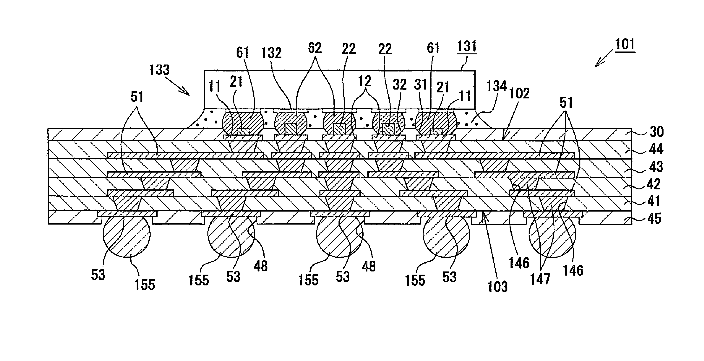
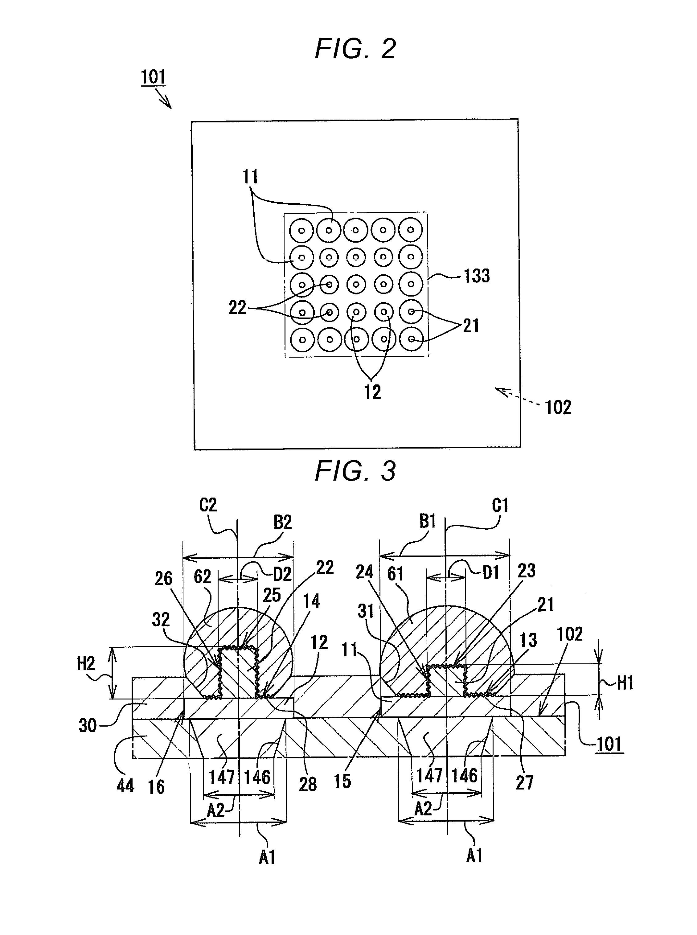
[0053]FIG. 1 is a schematic cross-sectional view showing a coreless wiring board 101 (wiring board) of the embodiment. The coreless wiring board 101 does not have a core board, and is a wiring board having a structure in which four resin insulating layers 41, 42, 43 and 44 made of an epoxy resin and conductor layers 51 made of copper are alternatively laminated. The resin insulating layers 41 to 44 are interlayer insulating layers having the same thickness and are made of the same material.

[0054]Furthermore, via holes 146 and via conductors 147 are provided respectively in each of the resin insulating layers 41 to 44. Each of the via holes 146 forms an inverted circular truncated cone shape, and the via holes are formed by carrying out a punching process using a YAG laser or a carbonate gas laser with respect to the respective resin insulating layers 41 to 44. Each of the via ...


PUM

PropertyMeasurementUnit
surface roughnessaaaaaaaaaa
surface roughness Raaaaaaaaaaa
outer diameter A2aaaaaaaaaa

Abstract

Embodiments provide a wiring board which is structured to be suitable for connection with components, whereby its reliability can be improved. An embodied wiring board of the invention has pads and a solder resist in which opening portions which expose the pads are formed. Protrusion-shaped members are fixed to some of the surfaces of the pads. The surfaces of the pads and the surfaces of the protrusion-shaped members are covered with solder bumps. The height of the solder bumps is larger than the height H1 and H2 of the protrusion-shaped members. The opening portions have different inner diameters, and the volume of the protrusion-shaped members increases as the diameter of the opening portion decreases.

Description

CROSS REFERENCE TO RELATED APPLICATIONS[0001]The present application claims priority from Japanese Patent Application No. 2011-277969, which was filed on Dec. 20, 2011, and Japanese Application No. 2012-244933, which was filed on Nov. 6, 2012, the disclosures of which are incorporated by reference in their entirety.BACKGROUND OF THE INVENTION[0002]1. Field of the Invention[0003]The present invention relates to a wiring board having a plurality of pads disposed in an electrode-forming area on the substrate main surface thereof and a method of manufacturing the same.[0004]2. Description of Related Art[0005]In the past, a wiring board formed by mounting components, such as IC chips (a so-called semiconductor package), was well known. As a structure for achieving electrical connection with IC chips, a structure in which solder bumps are formed on a plurality of connection terminals disposed on the bottom surface side of the IC chips or on a plurality of pads (so-called C4 pads: Controll...

Claims


Application Information

Patent Timeline
Patent Type & Authority Applications(United States)
IPC IPC(8): H05K1/11
CPCH05K1/111H01L24/14H01L2224/81192H01L2924/15311H05K1/113H05K3/4007H05K3/4682H05K2201/094H01L2924/01322H01L2924/1461H01L2224/1403H01L23/49816H01L23/49822H01L23/49838H01L2224/16225H01L2924/00H01L2224/13014H01L2224/1401H01L2224/16238H01L2924/12042H01L2924/00012
Inventor INOUE, MASAHIROSUGIMOTO, ATSUHIKO
Owner NGK SPARK PLUG CO LTD
Why Eureka
Try Eureka