Transition time lock loop with reference on request

a technology of transition time and lock loop, applied in the direction of pulse technique, voltage/temperature variation compensation, reliability increasing modifications, etc., can solve the problem that the general purpose input/output (gpio) circuitry may not be able to provide output signals that satisfy the transition time requirements, and the use of off-chip components is becoming more expensiv

Active Publication Date: 2013-07-25
QUALCOMM INC
View PDF3 Cites 3 Cited by
  • Summary
  • Abstract
  • Description
  • Claims
  • Application Information

AI Technical Summary

Benefits of technology

[0006]Aspects of the present disclosure include feedback circuitry configured to provide limited output slew rates across a wide range of output loads. The feedback circuitry locks output transition time regardless of the PVT proc...

Problems solved by technology

Output interface circuitry on a chip may include capacitive feedback, which compensates for some variations in load capacitance but may not be capable of meeting tight transition time specifications.
For interfaces that are designed to provide a limited output slew rate across a very wide range of output capacitive loads, general purpose input/output (GPIO) circuitry may not be able to provide output signals that satisfy the transition time requirements, even if such circuitry includes output drivers with capacitive feedb...

Method used


Image

  • Transition time lock loop with reference on request
  • Transition time lock loop with reference on request
  • Transition time lock loop with reference on request

Examples


Embodiment Construction

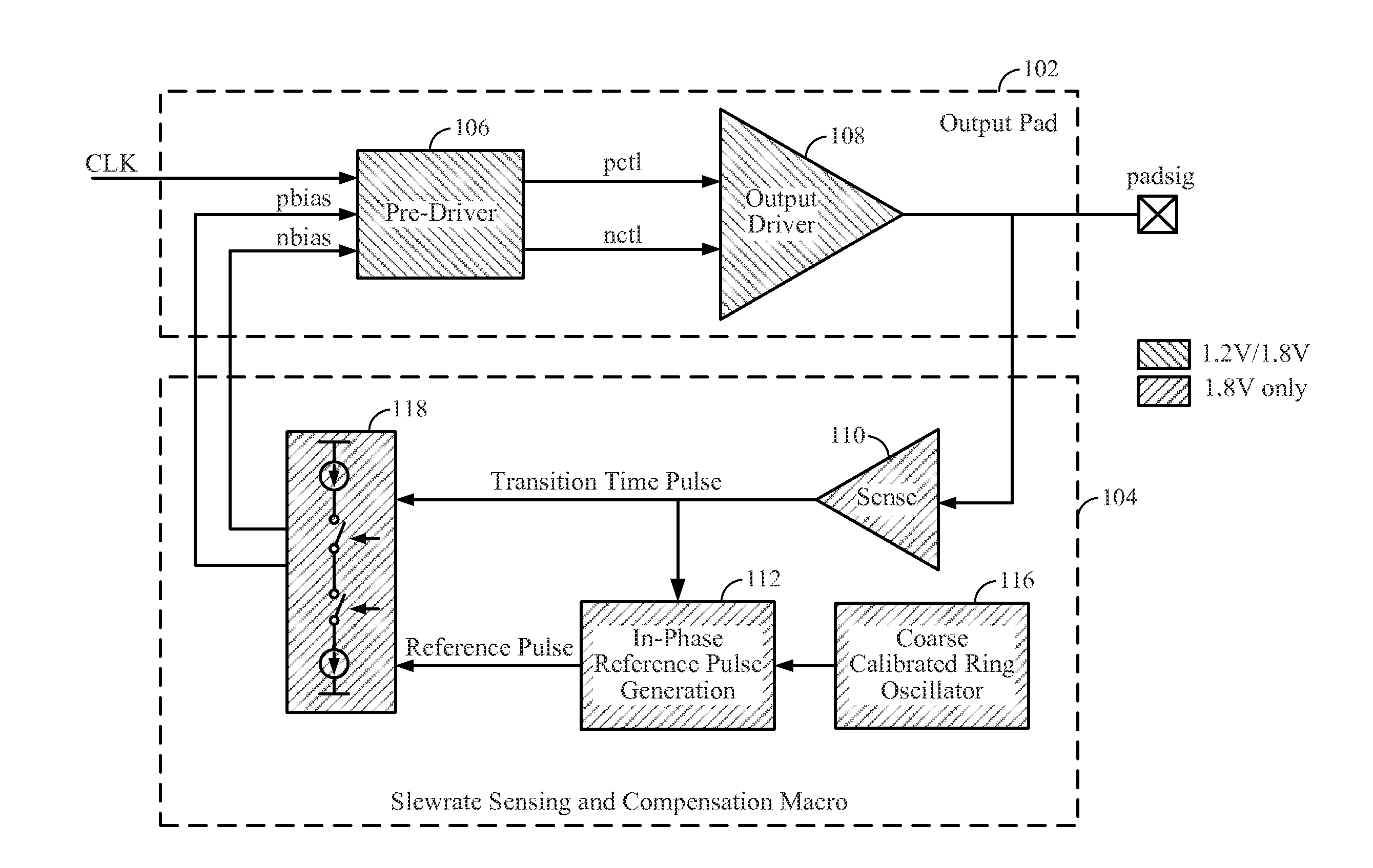
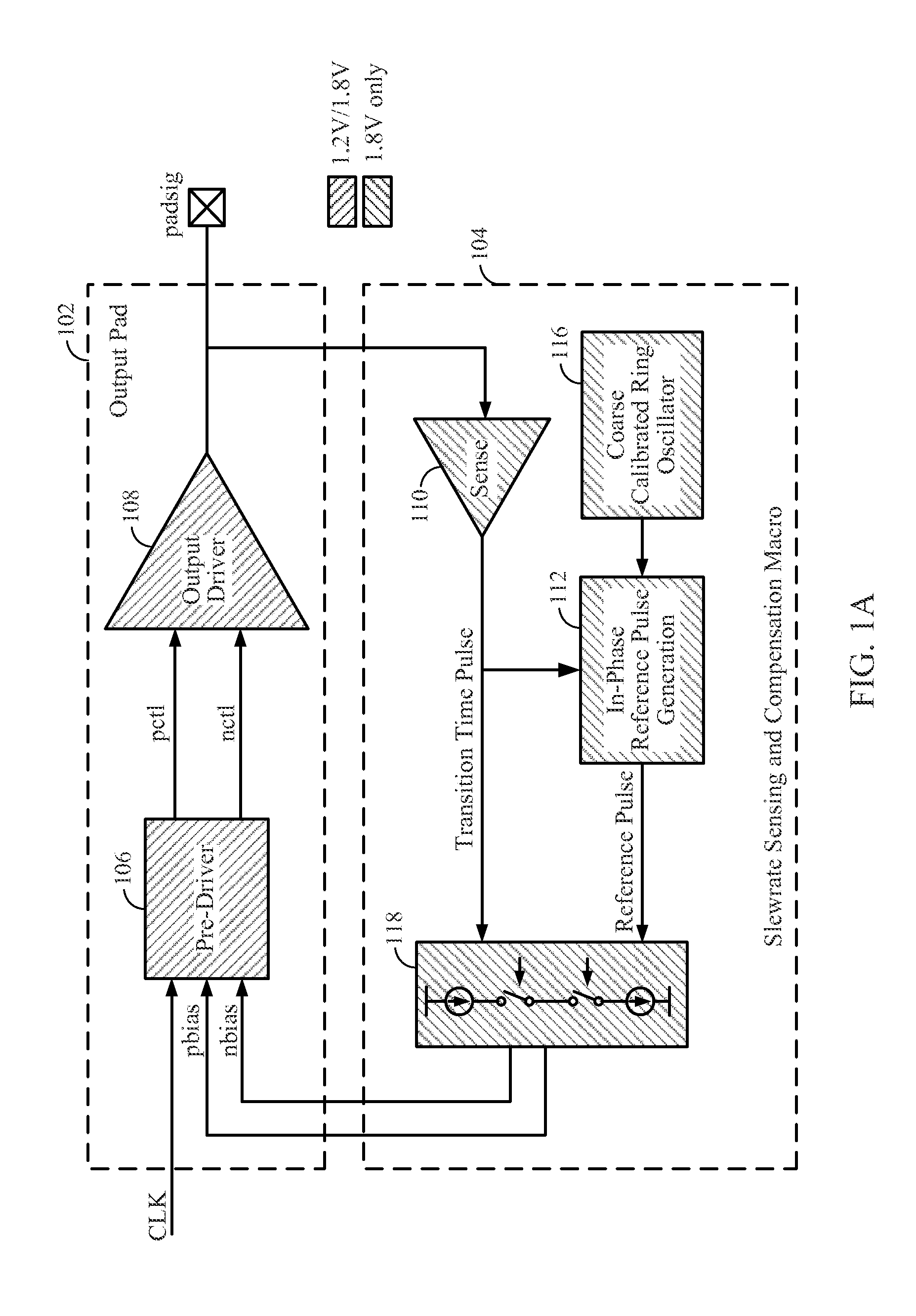
[0022]FIG. 1A shows a top level block diagram of a design architecture including circuitry 100 for locking output transition time according to aspects of the present disclosure. The circuitry 100 includes output pad circuitry 102 and slew rate sensing and compensation circuitry 104. According to aspects of the present disclosure, the output pad circuitry 102 is configured to support multiple output voltage domains. The output pad circuitry 102 includes a pre-driver 106 coupled to an output driver 108.

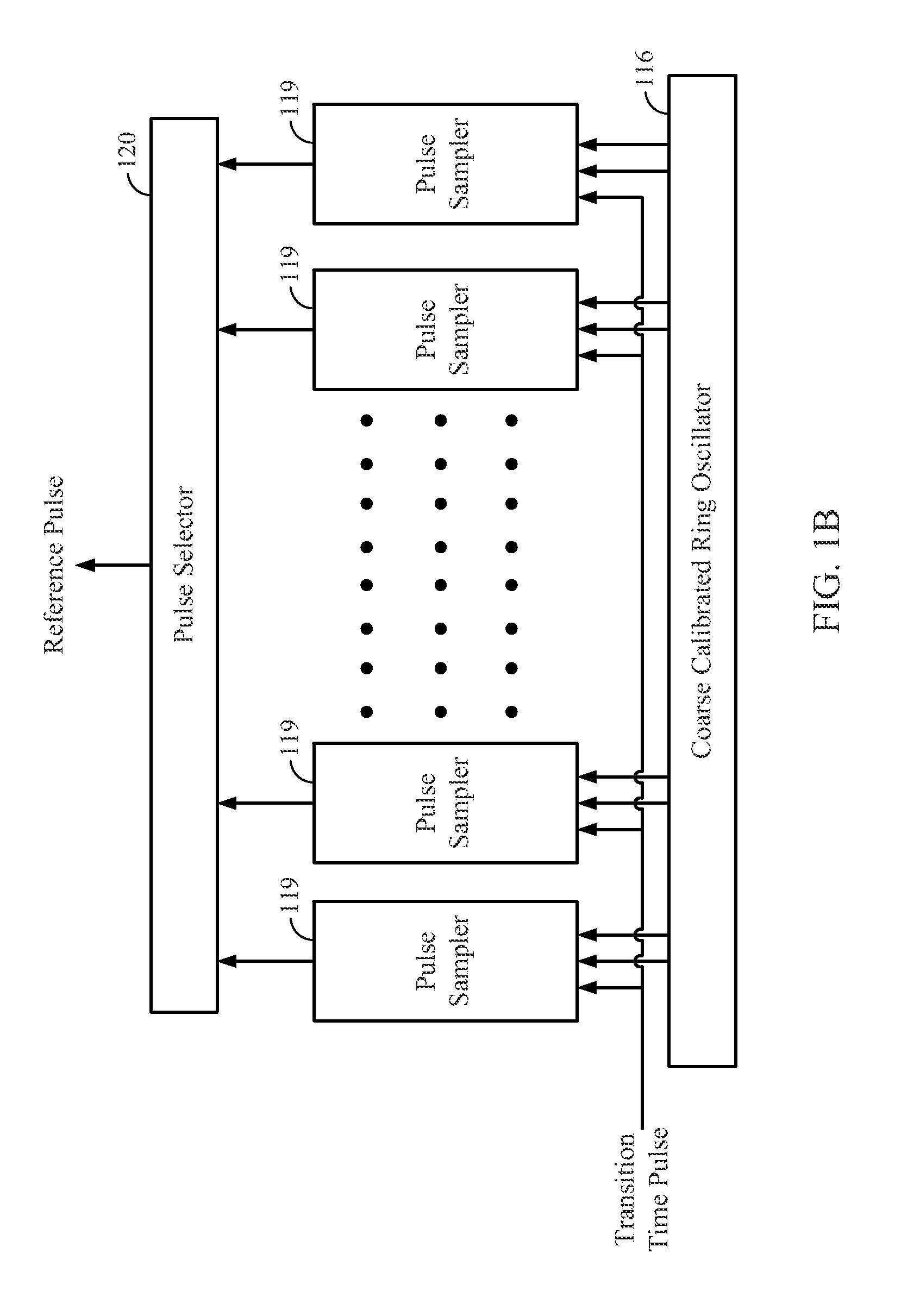
[0023]According to aspects of the present disclosure, slew rate sensing and compensation circuitry 104 is coupled in a feedback loop from an output node of the output driver 108 to inputs of the pre-driver 106. The slew rate sensing and compensation circuitry 104 includes sense circuitry 110 and in-phase reference pulse generation circuitry 112 coupled to bias generating circuitry 114. The slew rate sensing and compensation circuitry 104 also includes coarse calibrated ring oscillator c...


PUM


Abstract

Output driver feedback circuitry limits output slew rates across a wide range of output loads. A transition time lock loop architecture of the feedback circuitry compares a transition time pulse with a reference pulse to adjusts transition time of an output signal for various process-voltage-temperature (PVT) process corners, output voltage domains and output capacitances. Reference pulse generation circuitry provides a reference pulse in phase with the transition time pulse for each rise and fall of the output signal.

Description

CROSS REFERENCE TO RELATED APPLICATION[0001]The present application claims the benefit of U.S. Provisional Patent Application No. 61 / 588,717 to Chen et al. filed on Jan. 20, 2012.TECHNICAL FIELD[0002]The present disclosure relates generally to semiconductor output driver circuitry. More specifically, the present disclosure relates to controlling the transition time of an output from semiconductor output driver circuitry.BACKGROUND[0003]Integrated circuit design specifications generally include limits for the transition times and slew rates of output signals. For example, recent Mobile Industry Processor Interface (MIPI) input / output (I / O) interface standards, such as Serial Low-power Inter-chip Media Bus (SLIMBus), have called for limited output slew rates across a very wide range of output loads (e.g., 15 pF-75 pF) and across process, voltage and temperature (PVT) variations. Such standards also call for multiple output voltage modes.[0004]Variations in the load capacitance coupled...

Claims


Application Information

Patent Timeline
IPC IPC(8): H03L7/097
CPCH03K19/00384H03K19/00369
Inventor CHEN, WILSON J.TAN, CHIEW-GUAN
Owner QUALCOMM INC
Why Eureka
Try Eureka