Photoconversion device with enhanced photon absorption

a technology of photon absorption and conversion device, which is applied in the field of photoconversion device, can solve the problems of in-situ tunability of absorption spectrum of devices, and none of these technologies have enabled the conversion of absorbed light into electrical signals

Active Publication Date: 2013-08-01
FUNDACIO INST DE CIENCIES FOT NIQUES
View PDF1 Cites 46 Cited by
  • Summary
  • Abstract
  • Description
  • Claims
  • Application Information

AI Technical Summary

Benefits of technology

[0003]The present invention relates to photoconversion devices such as photovoltaic cells, photodetectors and light sources. In particular, the invention provides devices in which higher light absorption, or more efficient light emission can take place thanks to a single or multi-layer sheet of patterned and doped graphene. In addition, the devices of the invention also provide optimum thermal emission occurring at specific wavelengths that are selected by means of applied electric fields. And finally, it provides devices that utilize the infrared part of the solar spectrum to optimize conversion into electrical signals for improved solar cells.

Problems solved by technology

However, due to the specific material properties, none of these technologies have enabled conversion from absorbed light into electrical signals, or have been very inefficient as such.
Additionally, these devices did not exhibit in-situ tunability of the absorption spectrum, neither emission frequencies in the infrared or THz range.

Method used


Image

  • Photoconversion device with enhanced photon absorption
  • Photoconversion device with enhanced photon absorption
  • Photoconversion device with enhanced photon absorption

Examples


Embodiment Construction

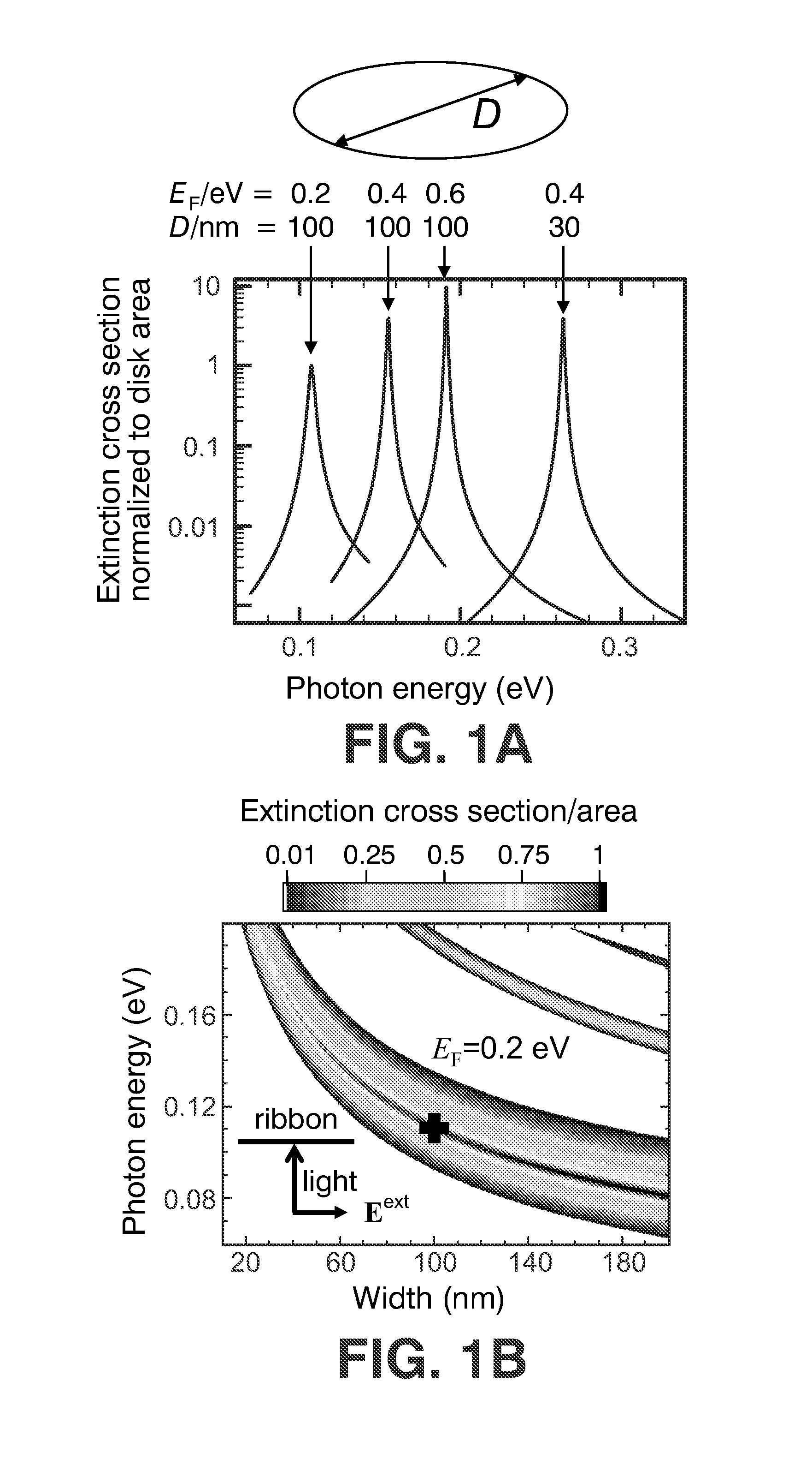
[0028]The individual graphene structures of the present invention are able to absorb light very efficiently. We show in FIG. 1 calculated results for the cross section of nanodisks and nanoribbons. These calculations, and the ones discussed below, are performed by solving Maxwell's equations using a realistic description of the graphene using the local random-phase approximation [F. H. L. Koppens, D. E. Chang, and F. J. Garcia de Abajo, Graphene Plasmonics: A Platform for Strong Light-Matter interactions, Nano Letters 11, 3370-3377 (2011)]. For disks (FIG. 1A), the diameter and Fermi energy (i.e., the level of doping) is indicated for each absorption spectrum. For ribbons (FIG. 1B), we represent the absorption cross section as a function of ribbon width for fixed Fermi energy (0.2 eV). The absorption cross section is defined as the effective area on which impinging light is absorbed. The plots here show a large increase in the absorption cross-section at specific light wavelengths c...


PUM


Abstract

An infrared photoconversion device comprising a collector with at least an active layer made of a single sheet of doped single-layer, bilayer, or multilayer graphene patterned as nanodisks or nanoribbons. The single sheet of doped graphene presents high absorbance and thus, the efficiency of devices such as photovoltaic cells, photodetectors, and light emission devices can be improved by using graphene as the central absorbing or emitting element. These devices become tunable because their peak absorption or emission wavelength is changed via electrostatic doping of the graphene.

Description

TECHNICAL FIELD[0001]The present invention relates to photoconversion devices such as photovoltaic cells, photodetectors and light sources.BACKGROUND OF INVENTION[0002]Light absorption plays a central role in optical detectors and photovoltaics. Inspired by nature, two different routes have been investigated to achieve perfect absorption. A first one consists in relying on diffusion in disordered lossy surfaces (e.g., black silver and carbon). Engineered materials have been synthesized following this solution to produce extraordinary broadband light absorption (e.g., dense arrays of carbon nanotubes). A second approach consists in using ordered periodic structures, as found in some nocturnal insects, where they produce the moth eye effect. This alternative has been pioneered by experimental and theoretical work showing total light absorption (TLA) in the visible using metallic gratings. In this context, the Salisbury screen (U.S. Pat. No. 2,599,944 B1), consisting of a thin absorbin...

Claims


Application Information

Patent Timeline
Patent Type & Authority Applications(United States)
IPC IPC(8): H01L31/0224B82Y99/00
CPCH01L31/02327H01L31/028H01L31/035209H01L31/06H01L31/09H01L31/0547Y02E10/547G01J3/28G01J5/10H01L31/0475Y02E10/52G01J5/046G01J5/0853
Inventor KOPPENS, FRANKGARCIA DE ABAJO, FRANCISCO JAVIER
Owner FUNDACIO INST DE CIENCIES FOT NIQUES
Why Eureka
Try Eureka