Light emitting diode device and method of producing the same

a technology of light-emitting diodes and diodes, which is applied in the direction of semiconductor/solid-state device manufacturing, semiconductor devices, electrical devices, etc., can solve the problems of easy damage to the optical semiconductor element, easy deformation and warpage of the encapsulating material (sheet), and easy non-uniform force on the optical semiconductor element under higher pressure, so as to achieve uniform forced pressure, reduce the effect of load applied to the device, and reduce the effect of heating tim

Inactive Publication Date: 2013-08-01
NITTO DENKO CORP
View PDF6 Cites 4 Cited by
  • Summary
  • Abstract
  • Description
  • Claims
  • Application Information

AI Technical Summary

Benefits of technology

[0019]Thus, a load applied to the device can be suppressed when pressure is higher and a heating time becomes longer.
[0020]Moreover, pressing with gas can achieve uniform forced pressure on the light emitting diode element under higher pressure. As a result, damages of the light emitting diode element and occurrence of voids in the encapsulating resin layer can be suppressed.

Problems solved by technology

In the method described in Japanese Unexamined Patent Publication No. 2011-228525A, however, since the encapsulating material is pressed and heated while being nipped by the press plates, the following problems may arise.
Moreover, the encapsulating material (sheet) may be deformed and warped or is easily damaged due to the pressure.
Moreover, in the vacuum press, forced pressure on the optical semiconductor element becomes easily non-uniform under higher pressure.
In this case, the optical semiconductor element may be damaged, or voids may be left in the encapsulating resin layer.

Method used


Image

  • Light emitting diode device and method of producing the same
  • Light emitting diode device and method of producing the same
  • Light emitting diode device and method of producing the same

Examples


preparation example 1

Preparation of Condensation / Addition Reaction Curing-Type Silicone Resin Composition

[0219]15.71 g (0.106 mol) of a vinyltrimetoxysilane (an ethylenical silicon compound) and 2.80 g (0.0118 mol) of a (3-glycidoxypropyl)trimethoxysilane (an epoxy group-containing silicon compound) were blended to 2031g (0.177 mol) of a polydimethylsiloxane containing silanol groups at both ends (a polydimethylsiloxane containing silanol groups at both ends, in general formula (1), all of the R1s are methyl, an average of n of 155, the number average molecular weight of 11,500, silanol group equivalent of 0.174 mmol / g), and they were stirred.

[0220]Here, the molar ratio (the number of moles of SiOH group / the total number of moles of SiOCH3 groups) of SiOH group of the polydimethylsiloxane containing silanol groups at both ends to SiOCH3 groups of the vinyltrimetoxysilane and the (3-glycidoxypropyl)trimethoxysilane was 1 / 1.

[0221]After stirring and mixing, 0.97 mL (0.766 g, a catalyst content: 0.88 mmol, ...

example 1

Preparation of Resin Composition

[0225]100 parts by mass of the thermosetting silicone resin compositions in Preparation Example 1 were blended with 26 pats by mass of YAG:Ce (a spherical shape, an average particle diameter of 10 μm) to prepare an encapsulating resin composition in a liquid state at room temperature.

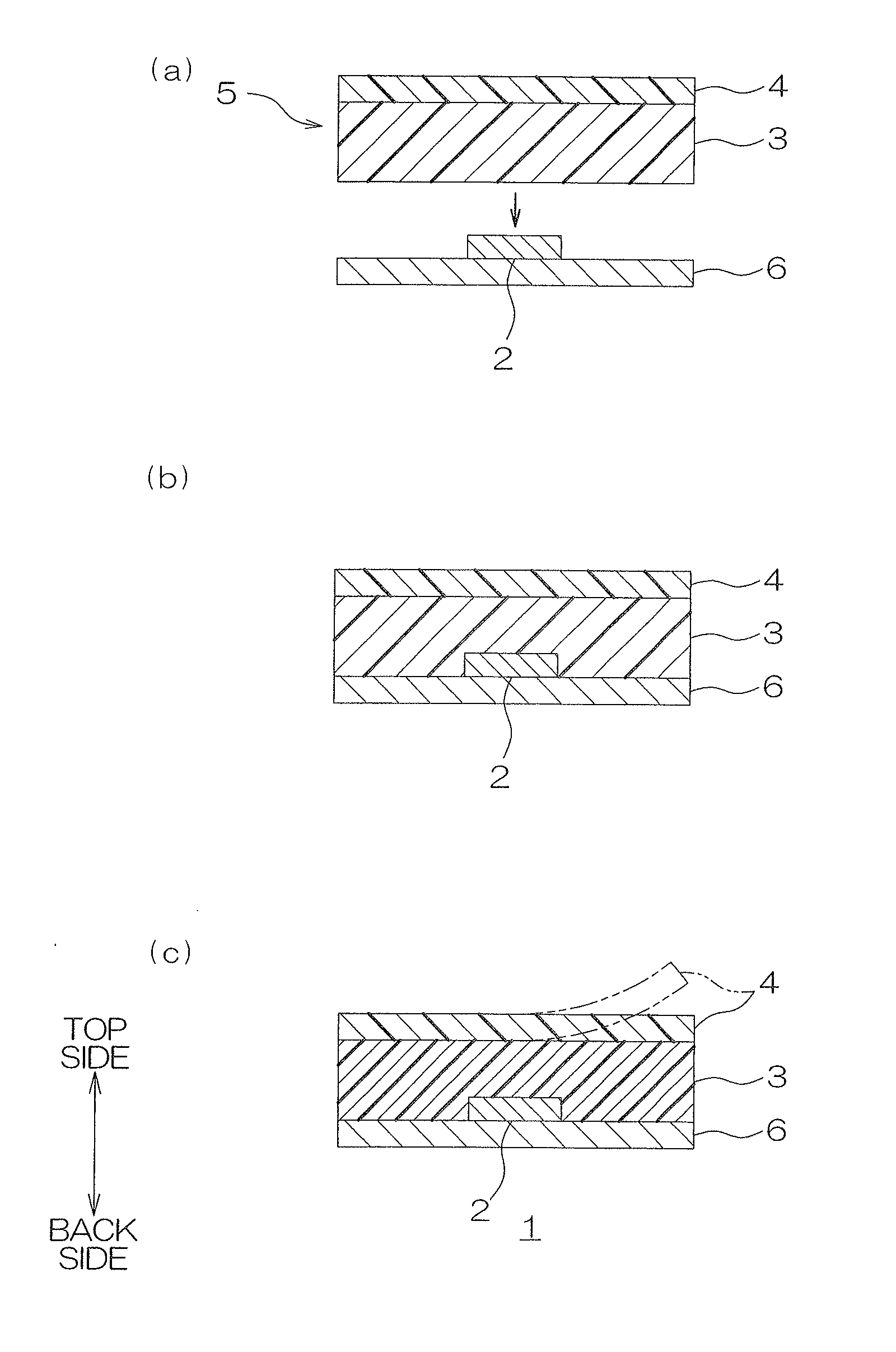
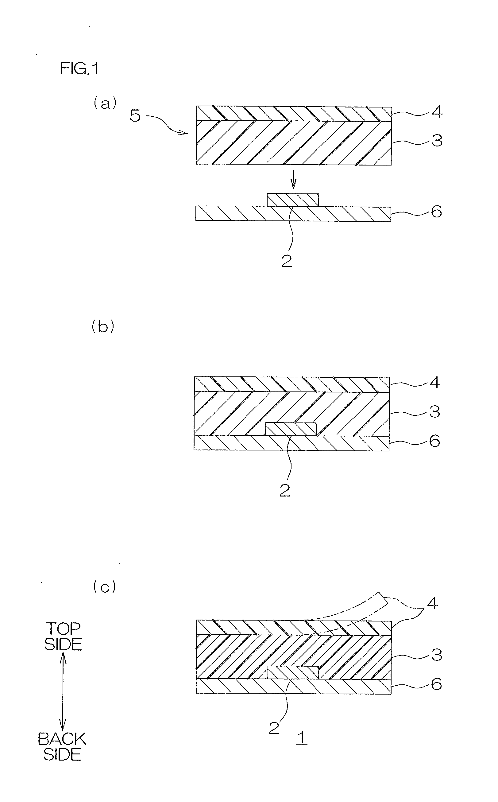
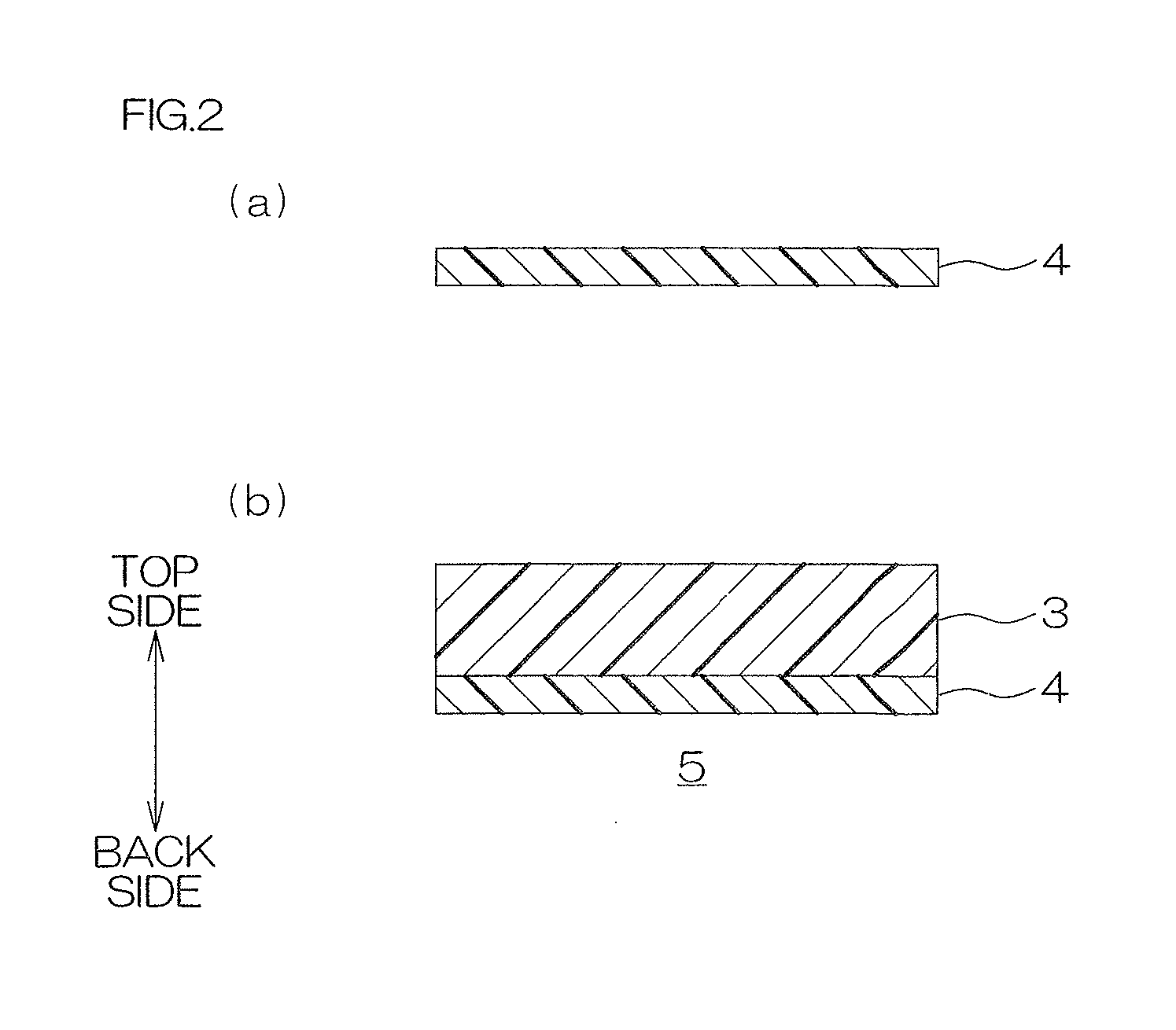
[0226]The prepared encapsulating resin composition was applied on an entire surface of a base substrate (see FIG. 2(a)) composed of a PET film using a doctor blade method, and then was heated at 135° C. for 20 minutes, so that an encapsulating sheet was prepared provided with the base substrate and an encapsulating resin layer in a B-stage having a thickness of 600 μm to be laminated on a surface of the base substrate (see FIG. 2(b)).

[0227]Subsequently, an encapsulating sheet was cut into a 5 cm square. Then the encapsulating sheet was positioned relative to the substrate having 25 blue light emitting diode elements (size of 0.35 mm×0.35 mm) mounted in the area of 5 cm sq...

example 2

[0232]The blue light emitting diode element was embedded in the encapsulating resin layer, and the encapsulating resin layer was completely cured and then the light emitting diode device was produced in the same manner as in Example 1 except for pressing at a room-temperature / reduced-pressure atmosphere using a vacuum press device instead of the press device in the embedding step.

[0233]The reduced pressure condition of the vacuum press device was 1 hPa (0.0001 MPa).


PUM

PropertyMeasurementUnit
thicknessaaaaaaaaaa
thicknessaaaaaaaaaa
compressive elasticity modulusaaaaaaaaaa

Abstract

A method of producing a light emitting diode device includes preparing an encapsulating resin layer; embedding a light emitting diode element in the encapsulating resin layer; and heating while pressing with gas the encapsulating resin layer having the light emitting diode element being embedded therein.

Description

CROSS-REFERENCE TO RELATED APPLICATION[0001]The present application claims priority from Japanese Patent Applications No. 2012-015796 filed on Jan. 27, 2012, the contents of which are hereby incorporated by reference into this application.BACKGROUND OF THE INVENTION[0002]1. Field of the Invention[0003]The present invention relates to a light emitting diode device and a method of producing the light emitting diode device. More particularly, the present invention relates to a light emitting diode device having a light emitting diode element being encapsulated by an encapsulating resin layer, and a method of producing the light emitting diode device.[0004]2. Description of Related Art[0005]It has been known that a light emitting diode device is produced through encapsulating a light emitting diode element (LED) by an encapsulating resin layer.[0006]For instance, the following method has been proposed. See, for example, Japanese Unexamined Patent Publication No. 2011-228525A.[0007]Speci...

Claims


Application Information

Patent Timeline
Patent Type & Authority Applications(United States)
IPC IPC(8): H01L33/52
CPCH01L33/52H01L33/56B29C43/18B29C43/10H01L2933/005H01L33/48
Inventor KATAYAMA, HIROYUKIOOYABU, YASUNARISATO, SATOSHI
Owner NITTO DENKO CORP
Why Eureka
Try Eureka