Method of producing liquid crystal display device

Active Publication Date: 2013-08-01
MERCK PATENT GMBH
View PDF11 Cites 31 Cited by
  • Summary
  • Abstract
  • Description
  • Claims
  • Application Information

AI Technical Summary

Benefits of technology

[0050]According to the present invention, a liquid crystal display device in which deterioration

Problems solved by technology

Furthermore, it is known that in a liquid crystal display device, when an electric double layer is generated between

Method used


Image

  • Method of producing liquid crystal display device
  • Method of producing liquid crystal display device
  • Method of producing liquid crystal display device

Examples


embodiment 1

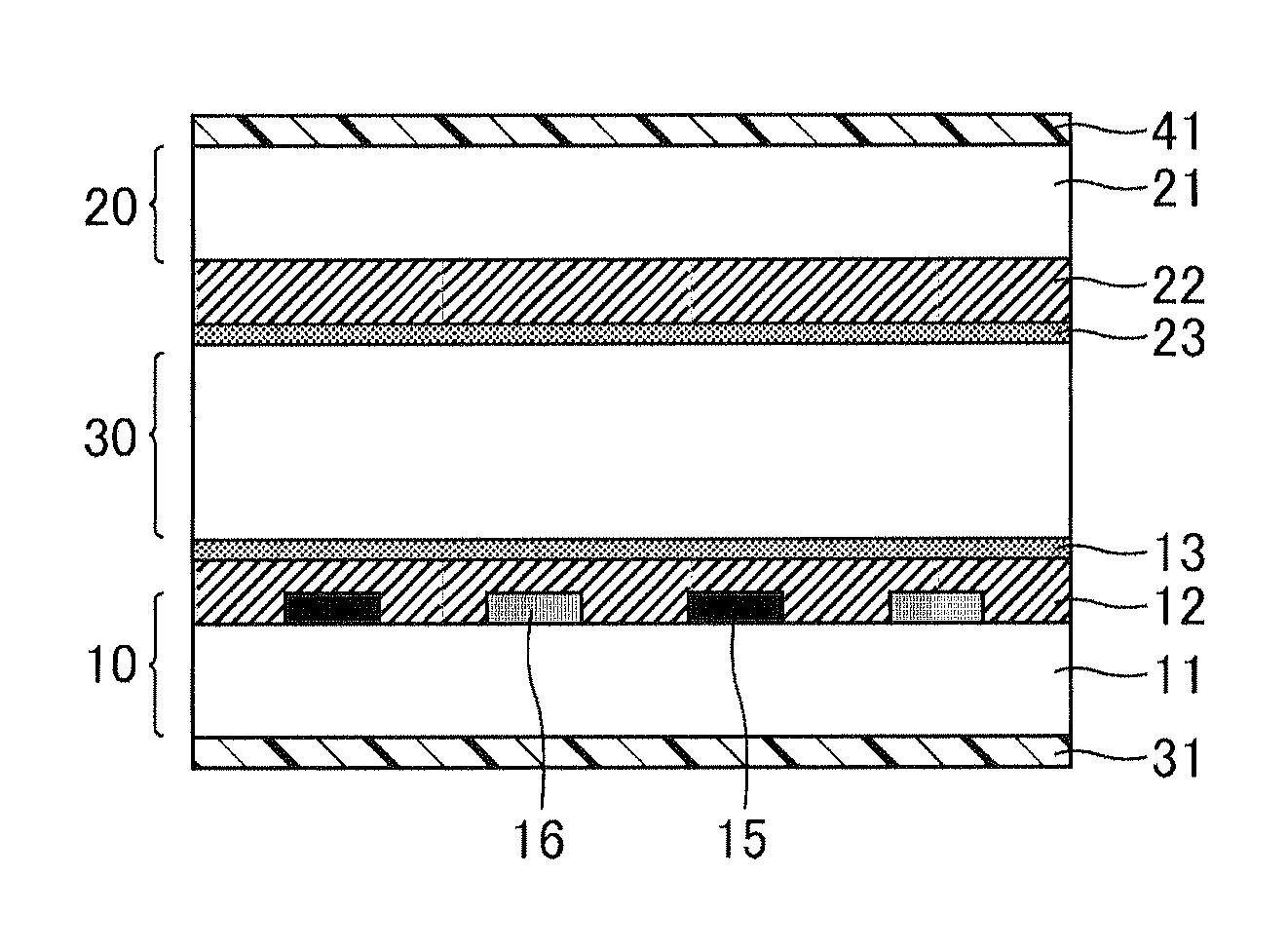
[0067]The method of producing a liquid crystal display device according to Embodiment 1 will be described in detail. The liquid crystal display device produced according to Embodiment 1 is a liquid crystal display device of the so-called IPS mode, and as illustrated in FIG. 1, pixel electrodes 15 and common electrodes 16 are extended approximately in parallel to each other, while the respective electrodes are formed in a zigzag form. Thereby, when an electric field is applied, the electric field vector is approximately perpendicular to the length direction of the electrodes, and therefore, a multi-domain structure is formed, while satisfactory viewing angle characteristics can be obtained. In addition, the pixel electrodes 15 and the common electrodes 16 may also be formed respectively in a linear form, instead of being formed in a zigzag form. The two arrows in FIG. 1 indicate the directions of irradiation polarization (in the case of using positive type liquid crystal molecules). ...

example 1

[0102]A glass substrate including a pair of combteeth electrodes (a pixel electrode and a common electrode) formed on the surface (combteeth electrode substrate) and a bare glass substrate (counter substrate) were prepared, and a polyvinyl cinnamate solution that serves as a material of a horizontal alignment film (varnish) was coated on each of the substrates by a spin coating method. As the material of the combteeth electrode, IZO was used. Furthermore, the electrode width L of the combteeth electrode was set to 3 μm, and the inter-electrode distance S was set to 9 μm. The polyvinyl cinnamate solution was prepared by dissolving polyvinyl cinnamate in an amount of 3 wt % in a solvent obtained by mixing equal amounts of N-methyl-2-pyrrolidone and ethylene glycol monobutyl ether.

[0103]The varnish was coated by a spin coating method, and then provisional drying was carried out at 90° C. for one minute. Subsequently, while nitrogen purging was carried out, burning was carried out at 20...

example 2

[0121]As shown in FIG. 8, a liquid crystal cell was produced in the same manner as in Example 1, except that a conductive film formed from ITO was formed on the respective surfaces on the opposite side of the liquid crystal layer side of the combteeth electrode substrate and the counter substrate. The conductive films were formed by a sputtering method. After bonding of the substrates, the cell surface was rubbed with a rayon cloth before the PS treatment, but static electricity charging did not occur. That is, there was no occurrence of alignment disorder and image sticking before the PS treatment.

[0122]From the above results, it was found that when a conductive film is formed, the influence of static electricity can be suppressed, and the generation of an electric double layer can be suppressed. In addition, also for the liquid crystal display device according to Example 2, the PS treatment is essential, as will be described in detail below, in order to suppress image sticking.

[01...


PUM


Abstract

The present invention provides a method of producing a liquid crystal display device which enables suppression of the occurrence of an electric double layer on a horizontal photo-alignment film before a polymer is formed, and exhibits reduced deterioration of display quality such as image sticking, or reduced display unevenness. The present invention is a method of producing a liquid crystal display device including the steps of (1) forming a liquid crystal layer containing a polymerizable monomer between a first substrate and a second substrate; (2) thermally annealing the liquid crystal layer at a temperature higher by 10° C. or more than the liquid crystalline phase-isotropic phase transition temperature of the liquid crystal layer; (3) forming horizontal alignment films to which the alignment treatment is performed by light irradiation on the first substrate and the second substrate by the time of the step (2); and (4) polymerizing the polymerizable monomer after the step (2).

Description

TECHNICAL FIELD[0001]The present invention relates to a method of producing a liquid crystal display device. More particularly, the present invention relates to a method of producing a liquid crystal display device by forming a polymer on a horizontal alignment film formed by a photo-alignment treatment.BACKGROUND ART[0002]A liquid crystal display (LCD) device is a display device which controls the transmission / shielding of light (on / off of the display) by controlling the alignment of liquid crystal molecules having birefringent properties. Examples of the display mode of LCD include a vertical alignment (VA) mode in which liquid crystal molecules having negative anisotropy of dielectric constant are vertically aligned with respect to the substrate surface; an in-plane switching (IPS) mode and a fringe field switching (FFS) mode in which liquid crystal molecules having positive or negative anisotropy of dielectric constant are horizontally aligned with respect to the substrate surfa...

Claims


Application Information

Patent Timeline
IPC IPC(8): G02F1/1337
CPCG02F1/1337G02F2001/133742G02F1/134363G02F1/133788G02F1/133742
Inventor MIYAKE, ISAMUMIYACHI, KOICHI
Owner MERCK PATENT GMBH
Why Eureka
Try Eureka