
RFID chip package and RFID tag

a chip package and chip technology, applied in the field of rfid chip packages, can solve the problems of difficult antenna design, difficult size reduction and band expansion, and achieve the effects of easy band expansion, increased flexibility in antenna design, and easy measurement of rfid chips

Inactive Publication Date: 2013-08-08
MURATA MFG CO LTD
View PDF6 Cites 30 Cited by
  • Summary
  • Abstract
  • Description
  • Claims
  • Application Information

AI Technical Summary

Benefits of technology

The present invention provides an RFID tag and chip package that can be easily matched to an antenna, even if the impedance of the antenna is low. This is achieved by using a reactance component of about -200 Ω for the input / output impedance of the RFID chip and a reactance component of about 0 Ω for the antenna. The power supply circuit is connected to the RFID chip, while the input / output impedance of the antenna is only a small value. This makes it easy to connect the RFID chip to different types of antennas and flexibility in antenna designing is increased. The impedance of the measuring system in measuring the RFID chip is preferably about 50 Ω, making the measurement of the RFID chip easy as well. The invention reduces the size of the RFID chip package and solves the difficulty in antenna designing problem.

Problems solved by technology

Thus, in the antenna, it is necessary to match its input / output impedance to the input / output impedance of the RFID chip, and hence antenna designing is difficult, and in particular, size reduction and band expansion are difficult.

Method used


Image

  • RFID chip package and RFID tag
  • RFID chip package and RFID tag
  • RFID chip package and RFID tag

Examples


Embodiment Construction

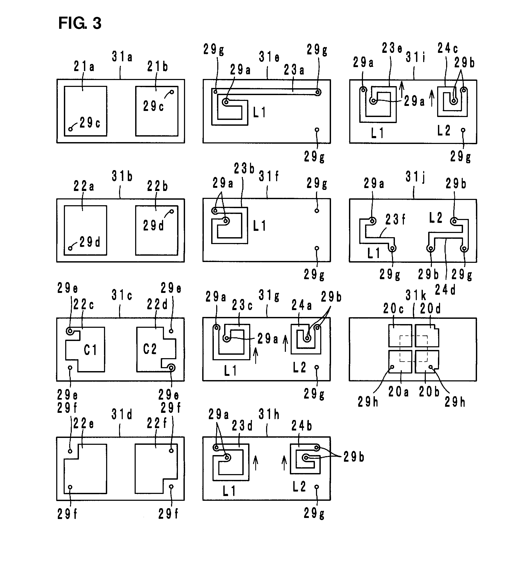
[0021]Hereinafter, preferred embodiments of an RFID chip package and an RFID tag according to the present invention will be described with reference to the accompanying drawings. It is noted that in the drawings, common elements and portions are denoted by the same reference signs, and the overlap description is omitted.

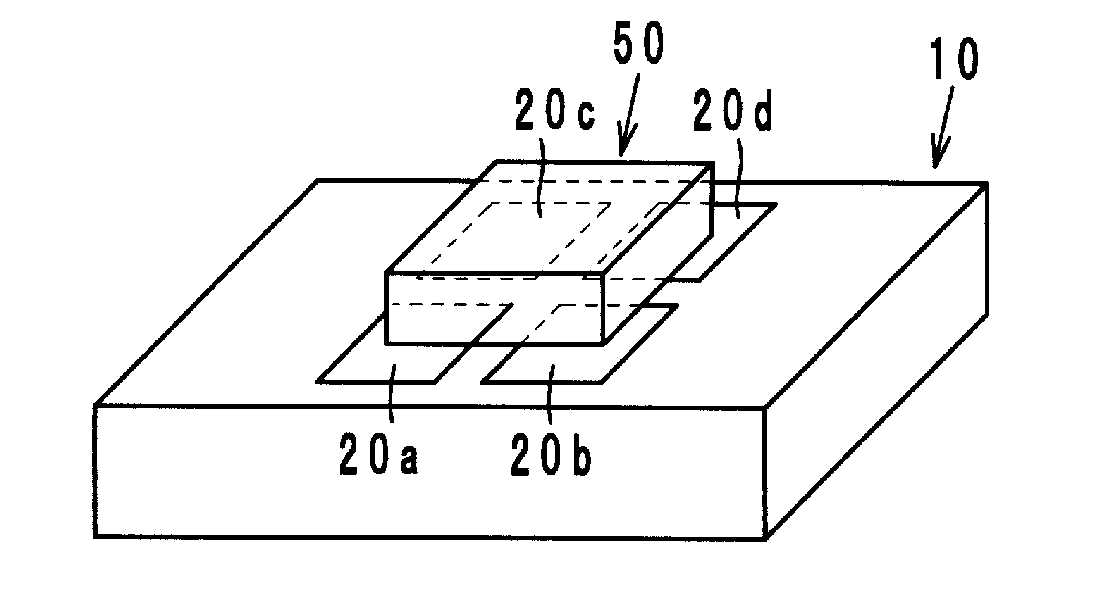
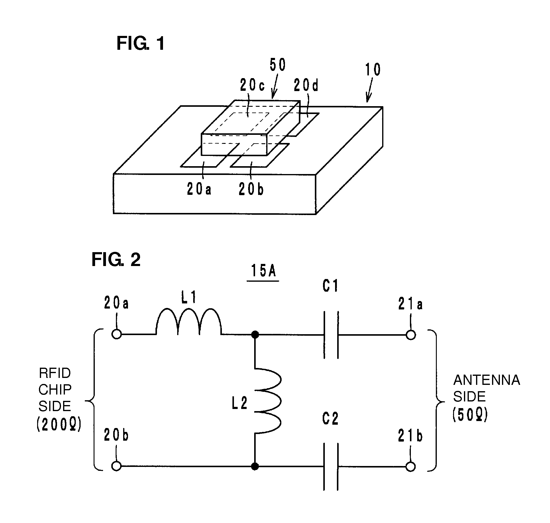
[0022]As shown in FIG. 1, in an RFID chip package according to a preferred embodiment of the present invention, an RFID chip 50 is mounted on a power supply circuit substrate 10 includes a laminate that includes a power supply circuit. It is noted that the RFID chip 50 may be incorporated in the power supply circuit substrate 10 or may be accommodated in a recess (not shown) provided in the substrate 10.

[0023]The RFID chip 50 preferably processes, for example, RF signals in the UHF band, includes a clock circuit, a logic circuit, a memory circuit, and the like, and has necessary information stored therein. In addition, the RFID chip 50 also preferably includes a volt...


PUM


Abstract

An RFID chip package includes an RFID chip including a voltage booster circuit and processing an RF signal in a UHF band and a power supply circuit connected to the RFID chip and including at least one inductance element. A reactance component of an input / output impedance at an antenna-connecting input / output terminal of the power supply circuit is substantially 0Ω.

Description

BACKGROUND OF THE INVENTION[0001]1. Field of the Invention[0002]The present invention relates to an RFID chip package, and in particular, relates to an RFID chip package interposed between an RFID chip and an antenna and an RFID tag in an RFID (Radio Frequency Identification) system.[0003]2. Description of the Related Art[0004]In recent years, an RFID system has been put into practical use as an article information management system, which includes a reader / writer that generates an induction field; and an RFID tag that is attached to an article, and non-contact communication using an electromagnetic field is established between the reader / writer and the RFID tag to transmit predetermined information therebetween. Here, the RFID tag is composed of an RFID chip that has stored predetermined information therein and processes a predetermined RF signal; and an antenna that performs transmission / reception of RF signals.[0005]Meanwhile, in the RFID system, since an RF signal is very weak, ...

Claims


Application Information

Patent Timeline
Patent Type & Authority Applications(United States)
IPC IPC(8): G06K19/07H04B5/48
CPCG06K19/07786H01Q1/2225G06K19/0723H01Q9/285H01Q7/00
Inventor DOKAI, YUYASHIROKI, KOJI
Owner MURATA MFG CO LTD
Learn More