Trench Formation Method For Releasing A Thin-Film Substrate From A Reusable Semiconductor Template

a technology of reusable semiconductors and trench formation methods, which is applied in the field of trench formation methods for releasing thin-film substrates from reusable semiconductor templates, and making semiconductor substrates, can solve the problems of inefficient removal, overheating variations, and no method is able to control the trench depth within the thin sacrificial layer

Active Publication Date: 2010-08-12
BEAMREACH SOLAR INC
View PDF99 Cites 38 Cited by
  • Summary
  • Abstract
  • Description
  • Claims
  • Application Information

AI Technical Summary

Benefits of technology

[0031]Therefore a need has arisen for trench formation methods which provides for an efficient and practical manufacturing method for releasing a 3-D thin-film semiconductor substrate from a 3-D template. The trench formation method must solve the depth control problems of known trench formation methods while also defining the boundary of the 3-D TFSS to be released and providing access to the buried porous sacrificial semiconductor layer.
[0033]In accordance with the disclosed subject matter, a method for forming a border definition trench to allow and aide the release of a 3-D TFSS from a re-usable template is provided that substantially eliminates or reduces disadvantages and problems associated with previously developed trench formation methods.
[0036]A technical advantage of the disclosed double-trench design is that the combination of shallow inner and deep outer trenches eliminates the difficulties of trench depth tolerance control. Thus, it is not required to precisely target the trench depth so that the trench bottom is in the thin porous silicon layer. As an example, in the case of 50 um thick epitaxial silicon grown on top of a 2 um thick porous silicon flat wafer surface area, the inner shallow trench may be cut into a depth of 25 um with a tolerance of + / −15 um, while the outer deep trench may be cut into a depth of 75 um with a tolerance of + / −20 um. With these laser cutting depth and tolerance requirements, many commercially available laser cutting / scribing systems may be used. Examples of commercially available lasers include but are not limited to NY:YAG lasers, Ar laser, Excimer lasers. Further, the beam of the lasers may be in pulsing modes or continuous mode. And the interaction between the laser beam and the silicon material may be in atmospheric ambient, in vacuum, in water jet, in silicon etching gas or solutions.

Problems solved by technology

As an example, saw blade cutting is to be avoided since it has to be started from the wafer edge and a drop-in saw may not be practical.
However none of these methods are able to control the trench depth within the thin sacrificial layer.
Using this laser cutter, the main technical challenge was the inefficient removal of silicon debris during laser cutting which caused local overheating variations.
As a result, the trench surfaces are rough and depth of the trench is difficult to control.
As an example, it is difficult to have a depth tolerance of less than + / −3 um for a 50 um deep trench cut.
Therefore, to cut the trench by laser to a depth within the thin porous silicon layer is not practical.
Third, the local charging will also cause surface roughness and form grass-like silicon microstructures at trench bottom, as visible in FIG. 4.
The challenge of using laser cutting / scribing for making border definition trenches that do not cut through the wafer is the control of trench depth.
To make a narrow trench and stop the trench bottom within the buried thin porous silicon layer, no more no less, is not practical given the state of art laser machining technologies.
However, these issues may affect process controls in subsequent template re-use cycle.
The TFSS film (epitaxial silicon) thickness variation is another factor that makes trench depth control difficult.
In addition to the above factors, the wafer non-flatness, or bowing, may also cause difficulties for trench depth control.
As an example, when laser cutting is used, the non-flatness will cause difficulty of the laser beam focusing control, which results in poor trench depth and surface control.

Method used


Image

  • Trench Formation Method For Releasing A Thin-Film Substrate From A Reusable Semiconductor Template
  • Trench Formation Method For Releasing A Thin-Film Substrate From A Reusable Semiconductor Template
  • Trench Formation Method For Releasing A Thin-Film Substrate From A Reusable Semiconductor Template

Examples


Embodiment Construction

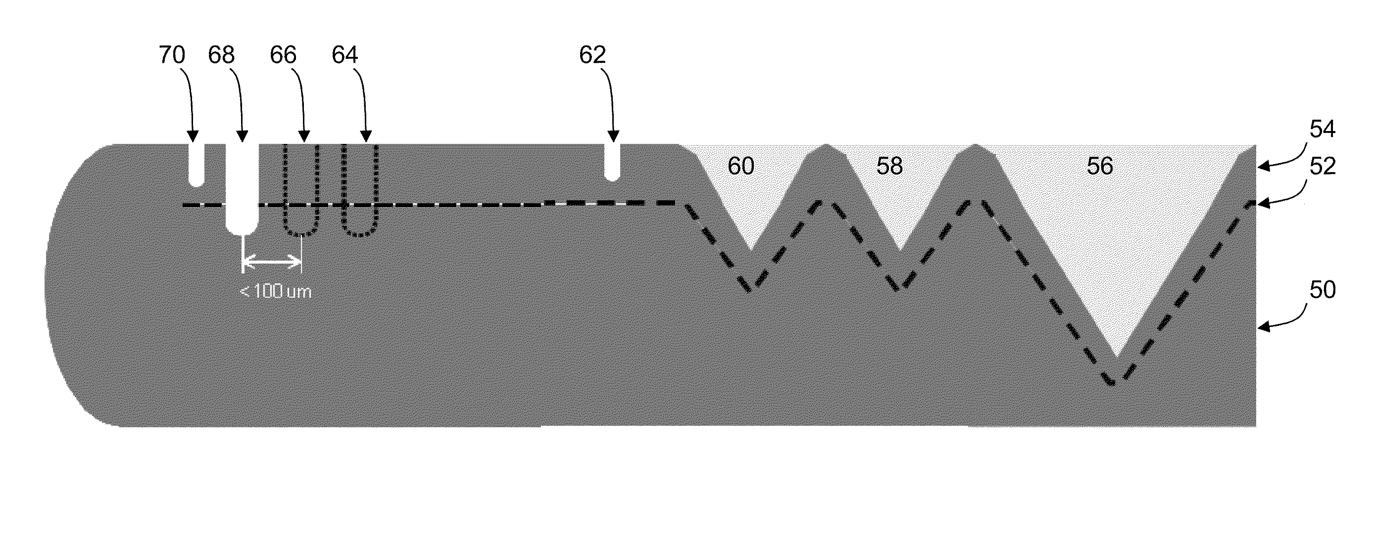
[0053]The following description is not to be taken in a limiting sense, but is made for the purpose of describing the general principles of the present disclosure. The scope of the present disclosure should be determined with reference to the claims. And although described with reference to the manufacture of a thin-film silicon substrate, a person skilled in the art could apply the principles discussed herein to any semiconductor material and the manufacture of a substantially planar or a 3-D thin-film semiconductor substrate. Exemplary embodiments of the present disclosure are illustrated in the drawings, like numbers being used to refer to like and corresponding parts of the various drawings.

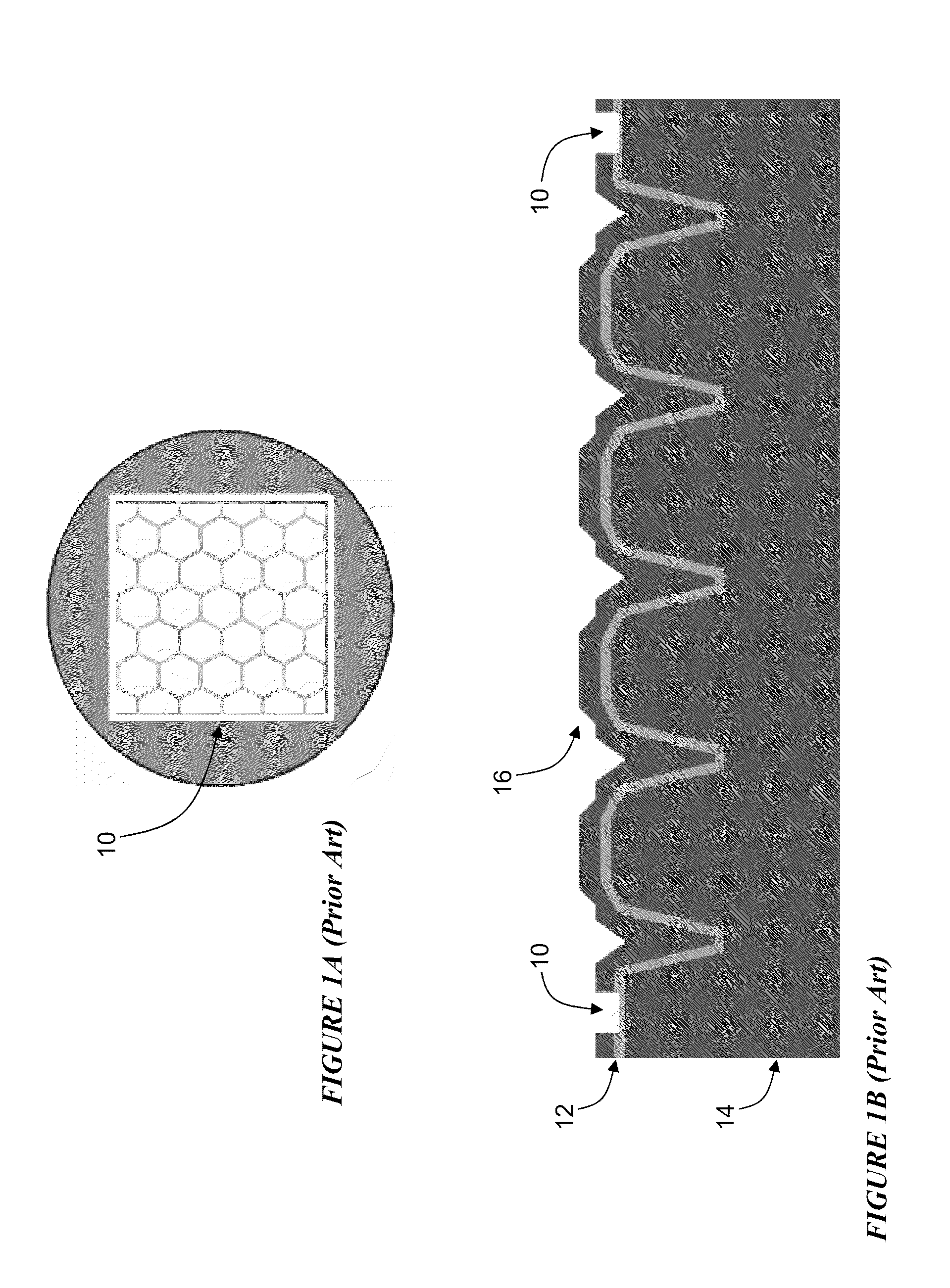
[0054]FIGS. 1A and 1B illustrate a self-supporting three-dimensional honey-comb prism thin-film silicon substrate (3-D TFSS) according to U.S. application Ser. No. 11 / 868,489 (U.S. Patent Pub. No. 2008 / 0264477A1).

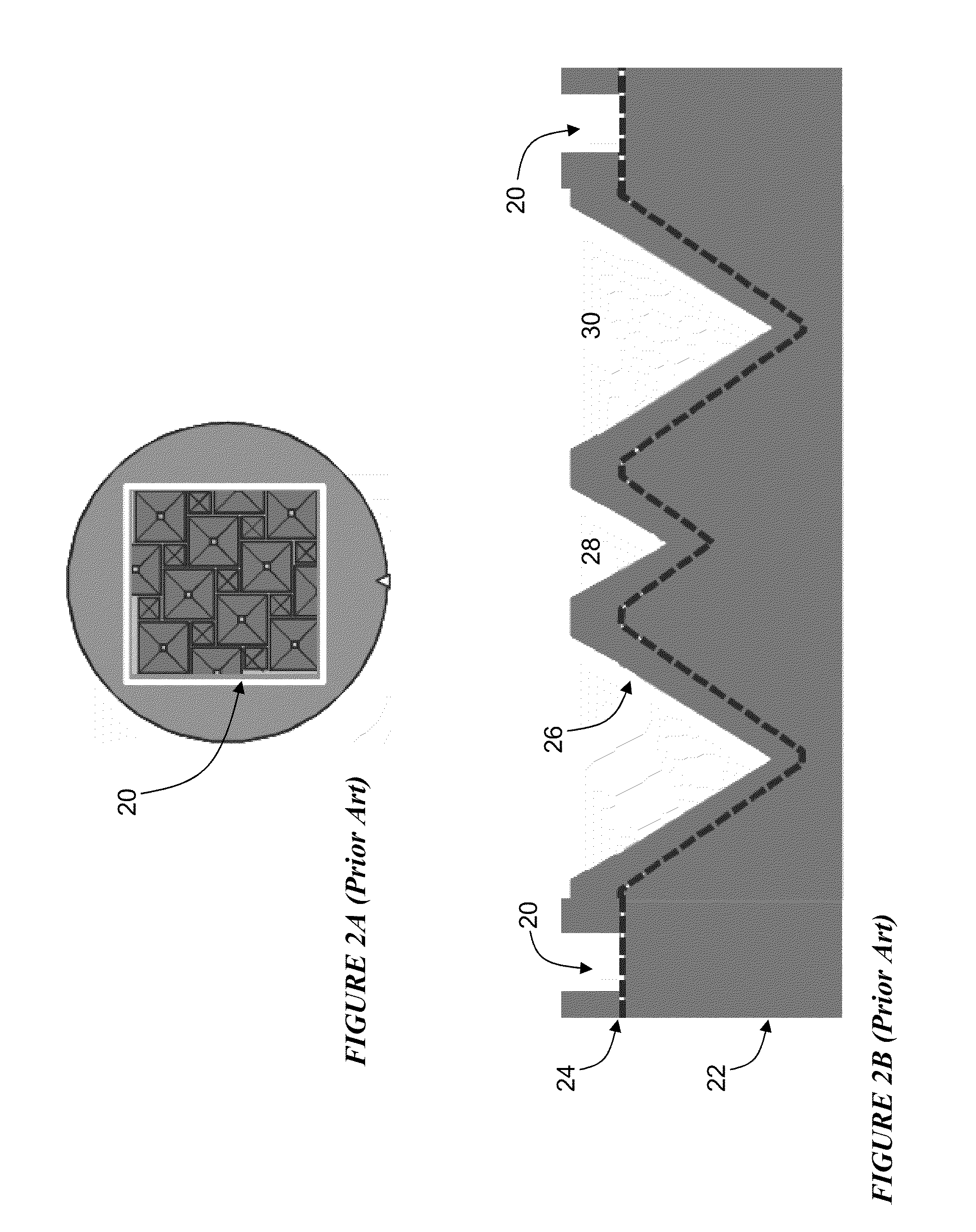
[0055]FIGS. 2A and 2B illustrate schematic drawings of an alternate 3-D TFSS des...


PUM


Abstract

A method is provided for fabricating a thin-film semiconductor substrate by forming a porous semiconductor layer conformally on a reusable semiconductor template and then forming a thin-film semiconductor substrate conformally on the porous semiconductor layer. An inner trench having a depth less than the thickness of the thin-film semiconductor substrate is formed on the thin-film semiconductor substrate. An outer trench providing access to the porous semiconductor layer is formed on the thin-film semiconductor substrate and is positioned between the inner trench and the edge of the thin-film semiconductor substrate. The thin-film semiconductor substrate is then released from the reusable semiconductor template.

Description

[0001]This application claims the benefit of provisional patent application Ser. No. 61 / 150,392 filed on Feb. 6, 2009, which is hereby incorporated by reference.[0002]This application incorporates by reference the co-pending patent application entitled “METHODS FOR MANUFACTURING THREE-DIMENSIONAL THIN-FILM SOLAR CELLS”, U.S. application Ser. No. 11 / 868,489 (U.S. Patent Pub. No. 2008 / 0264477A1) by Mehrdad Moslehi and filed on Oct. 6, 2007, and is incorporated herein by reference as if fully set forth herein.[0003]This application incorporates by reference the co-pending patent application entitled “SUBSTRATE RELEASE METHODS AND APPARATUS”, U.S. application Ser. No. 12 / 473,811 (U.S. Patent Pub. No. 2010 / 0022074A1) by David Wang filed and on Apr. 28, 2009, and is incorporated herein by reference as if fully set forth herein.FIELD[0004]This disclosure relates in general to the fields of semiconductor microelectronics, micro-electro-mechanical systems (MESM, photovoltaics and solar cells...

Claims


Application Information

Patent Timeline
Patent Type & Authority Applications(United States)
IPC IPC(8): H01L21/20
CPCH01L21/76229H01L21/76232Y02E10/547H01L31/03529H01L31/1804H01L31/035281Y02P70/50
Inventor WANG, DAVID XUAN-QIMOSLEHI, MEHRDAD
Owner BEAMREACH SOLAR INC
Why Eureka
Try Eureka