PCB having individual reflective structure and method for manufacturing light emitting diode package using the same

a technology of reflective structure and printed circuit board, which is applied in the manufacture of printed circuits, printed circuit aspects, circuit optical details, etc., can solve the problems of complex manufacturing process increased manufacturing costs of light emitting diodes, and inability to manufacture light emitting diodes exclusively by single manufacturers

Inactive Publication Date: 2013-08-08
EG LITEC CO LTD +1
View PDF0 Cites 9 Cited by
  • Summary
  • Abstract
  • Description
  • Claims
  • Application Information

AI Technical Summary

Benefits of technology

[0027]The present invention has been made in an effort to solve the above-described problems associated with prior art, and an object of the present invention is to provide a PCB having an individual reflective structure and a method for manufacturing an LED package using the same, which can prevent reabsorption of light between LED chips by providing an individual reflective structure between the LED chips when the LED package is configured using two or more LED chips.

Problems solved by technology

That is, the light emitting diode cannot be exclusively manufactured by a single manufacturer but can be manufactured through the cooperation of other manufacturers.
Thus, the manufacturing process of the light emitting diode unit is complicated and the manufacturing costs of the light emitting diode unit are increased, which is problematic.
Thus, the overall thickness of the light emitting diode unit is increased, which is an obstacle to thinning of an electronic product employing the light emitting diode unit.
As a result, the overall thickness of the light emitting diode unit is increased, which is an obstacle to thinning of an electronic product employing the light emitting diode unit.
The light emitting diode unit of the prior art has limitations in improving the wavelength conversion efficiency of emitted light, and thus it is difficult to increase the light output, brightness, or color rendering.
However, according to this type of light emitting diode package, when two or more light emitting diode chips are mounted in the reflective groove, the light output may be reduced due to reabsorption of light between adjacent light emitting diode chips.
However, it is impossible to directly plate the Cu layer with silver, and thus a nickel (Ni) layer is formed on the Cu layer by plating as a buffer layer for Ag plating.

Method used


Image

  • PCB having individual reflective structure and method for manufacturing light emitting diode package using the same
  • PCB having individual reflective structure and method for manufacturing light emitting diode package using the same
  • PCB having individual reflective structure and method for manufacturing light emitting diode package using the same

Examples


Embodiment Construction

[0052]Hereinafter, preferred embodiments of a PCB having an individual reflective structure and a method for manufacturing an LED package using the same according to the present invention will be described in detail with reference to the accompanying drawings.

[0053]Features and advantages of the PCB having an individual reflective structure and the method for manufacturing an LED package using the same according to the present invention will be apparent from the following detailed description of the preferred embodiment of the present invention.

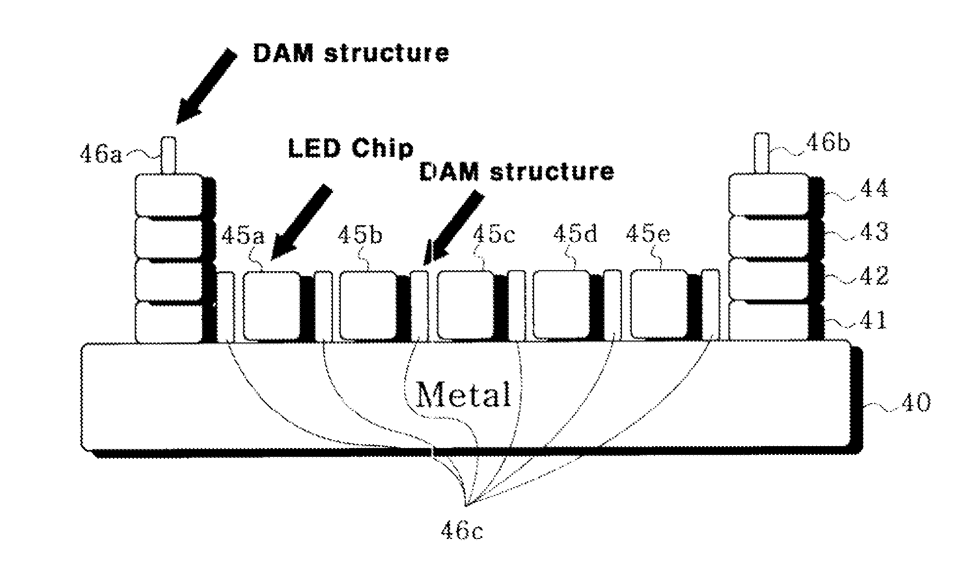
[0054]FIG. 3 is a schematic diagram showing the configuration of a chip-on-board (COB) & chip-on-heat-sink (COH) type light emitting diode package in accordance with an exemplary embodiment of the present invention, and FIG. 4 is a schematic diagram showing the configuration of a chip-on-metal (COM) type light emitting diode package in accordance with another exemplary embodiment of the present invention.

[0055]The present invention provides a...


PUM


Abstract

A printed circuit board (PCB) having an individual reflective structure and a method for manufacturing a light emitting diode (LED) package using the same, which can prevent reabsorption of light between LED chips by providing an individual reflective structure between the LED chips when the LED package is configured using two or more LED chips. The PCB includes a PCB; a wiring pattern-forming material layer formed on the PCB with an insulating layer interposed therebetween; dams formed on the wiring pattern-forming layer around chip mounting areas of the PCB; and a light reabsorption prevention dam formed on the wiring pattern-forming material layer between the chip mounting areas where LED chips are mounted.

Description

CROSS-REFERENCE TO RELATED PATENT APPLICATION[0001]This application claims the benefit of Korean Patent Application No. 10-2012-0011927, filed on Feb. 6, 2012, it the Korean Intellectual Property Office, the disclosure of which is incorporated herein in its entirety by reference.BACKGROUND OF THE INVENTION[0002]1. Field of the Invention[0003]The present invention relates to a light emitting diode (LED) package and, more particularly, to a printed circuit board (PCB) having an individual reflective structure and a method for manufacturing an LED package using the same, which can prevent reabsorption of light between LED chips by providing an individual reflective structure between the LED chips when the LED package is configured using two or more LED chips.[0004]2. Description of the Related Art[0005]A light emitting diode is an electronic device that produces minority carriers (electrons or holes) injected using p-n junctions in semiconductors and emits light by recombination of the...

Claims


Application Information

Patent Timeline
Patent Type & Authority Applications(United States)
IPC IPC(8): H01L33/08H01L33/60
CPCH01L25/0753H01L33/60H05K2201/09909H01L2924/00014H01L2224/92247H01L2224/85439H01L2224/83439H01L2224/73265H01L2224/4912H01L2224/49113H01L2224/48227H01L2224/48108H01L2224/48091H01L2224/32225H05K1/0274H01L24/92H05K1/021H05K1/181H05K3/325H05K2201/0338H05K2201/10106H05K2201/2054H05K2203/072H01L2924/12041H01L2224/4805H01L2224/4909H01L24/32H01L24/48H01L24/49H01L24/83H01L24/85H01L2224/45099H01L2224/29099H01L2924/00H01L2224/48137H01L33/48
Inventor JANG, JONG-JIN
Owner EG LITEC CO LTD
Why Eureka
Try Eureka