High speed backplane connector

a backplane connector, high-speed technology, applied in the direction of coupling device connection, coupling device details, printed circuits, etc., can solve the problems of affecting signal performance or creating impedance mismatch, large pitch used, and complex structure, so as to improve the performance of existing backplane connector sets, increase interconnect density, and reduce costs

Inactive Publication Date: 2013-08-08
HSIO TECH
View PDF2 Cites 79 Cited by
  • Summary
  • Abstract
  • Description
  • Claims
  • Application Information

AI Technical Summary

Benefits of technology

[0009]The present disclosure is directed to a high speed backplane connector (“HSBC”) that will enable next generation electrical performance. The present disclosure improves the performance of existing backplane connector sets by leveraging alternate manufacturing techniques to reduce cost and provide an opportunity to increase interconnect density. The present backplane connector is a drop in replacement for existing products, with an evolutionary road map to higher performance and increased density, while enabling an overall system cost reduction.

Problems solved by technology

The compliant tails used for mounting along with the via required for insertion are parasitic and can disrupt signal performance or create an impedance mismatch.
The contact structures can be extremely long relatively speaking due to the need to change directions for lateral to vertical or right angle interfaces, and the pitches used are relatively large due to a variety of mechanical and electrical issues.
The use of an intermediate connector between the backplane connector and the PCB also has parasitic effects that can disrupt signal performance or create an impedance mismatch.
These contact families are also relatively expensive due to the large material content and relatively sophisticated design and tooling requirements.
The PCB's used with these solder ball style attachments are often large, with many layers and consequently very expensive compared to thinner PCB's with fewer layers.
As system architectures evolve, the environment these types of connectors operate in will become increasingly complex with a huge expansion in bandwidth and speed requirements.
Existing products can meet today's electrical performance needs with relatively expensive connector products and sophisticated system and circuit board designs.

Method used


Image

  • High speed backplane connector
  • High speed backplane connector
  • High speed backplane connector

Examples


Embodiment Construction

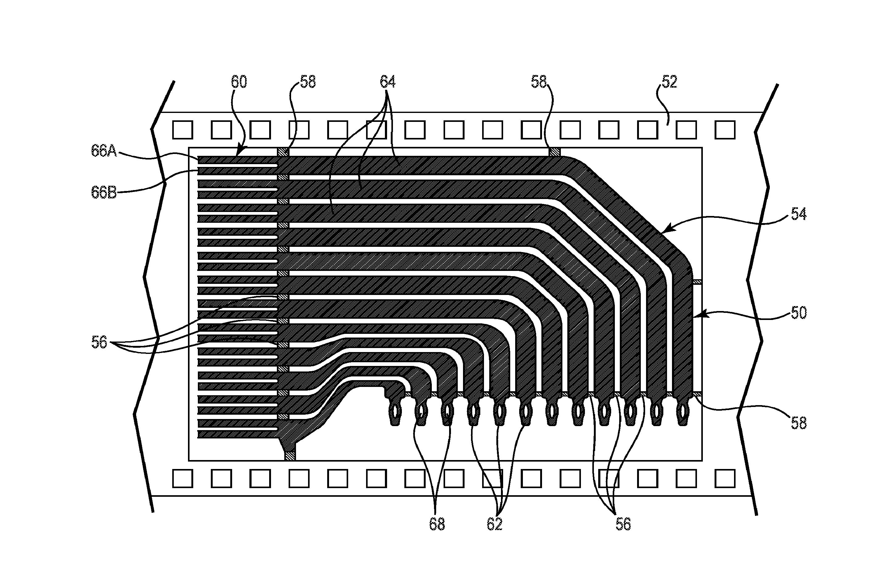
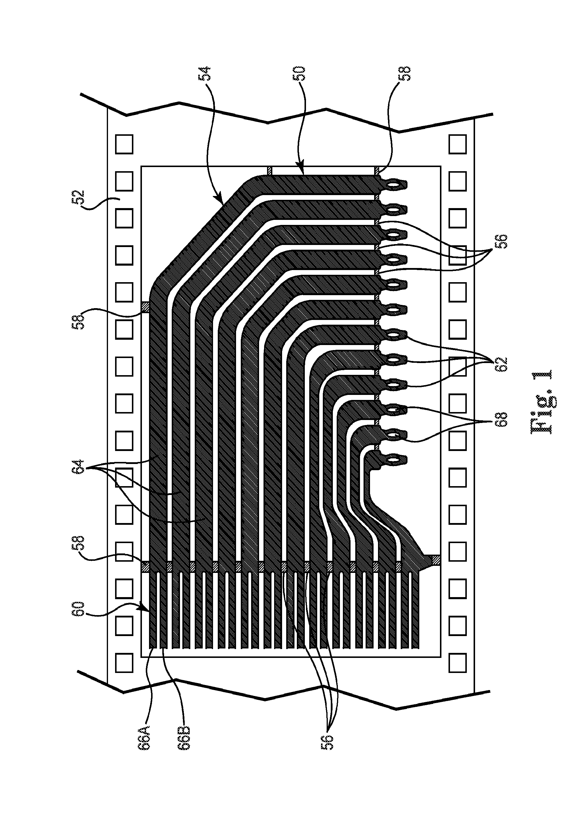
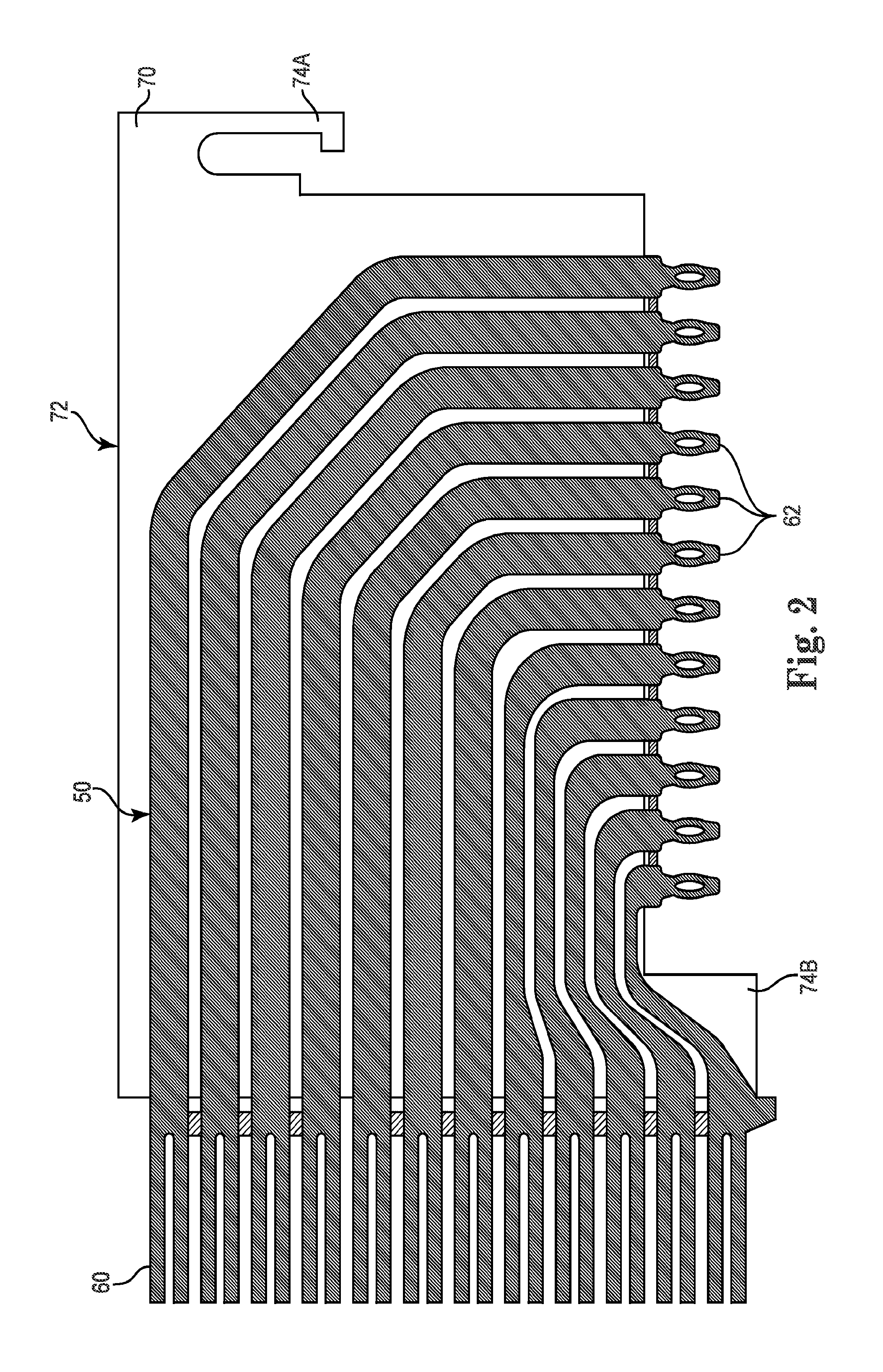
[0043]FIG. 1 illustrates a backplane connector set 50 attached to carrier 52 in accordance with an embodiment of the present disclosure. Interconnect elements 54 and tie bars 56 are created by etching or blanking as a group. The tie bars 56 retain the individual interconnect elements 54 in the desired position. Tie bars 58 retain the entire connector set 50 to the carrier 52 during the early steps of this process. The backplane connector set 50 is optionally plated.

[0044]In the illustrated embodiment, each interconnect element 54 includes contact members 60, 62 electrically coupled by conductive traces 64. The contact members 60 include a pair of beams 66A, 66B (“66”) formed during the etching or blanking process. Contact members 62 include elongated center opening 68 that permits elastic deformation during insertion into a via in a PCB. In the illustrate embodiment, the contact members 60 are oriented at a right angle relative to the contact members 62. A variety of other contact s...


PUM

PropertyMeasurementUnit
aspect ratioaaaaaaaaaa

Abstract

A backplane connector including a substrate and a backplane connector set attached to the substrate. The backplane connector set includes a plurality of interconnect elements each having a conductive trace, a first contact member, and a second contact members matched to the first contact member. The first and second contact members extend beyond perimeter edges of the substrate. A plurality of conductive tie bars retain the interconnect elements in a fixed relationship prior to attachment to the substrate. Additive printing processes can be used to form the conductive traces.

Description

TECHNICAL FIELD[0001]The present application relates to a high performance electrical interconnect between one printed circuit board (“PCB”) and another printed circuit board. The present disclosure improves the performance of existing backplane connector sets by leveraging alternate manufacturing techniques to reduce cost and provide an opportunity to increase interconnect density.BACKGROUND OF THE INVENTION[0002]System architectures for data, communications, industrial, and instrumentation applications often include two or more printed circuit boards electrically couple with a backplane connector. Backplane connectors typically include a plurality of conductive traces each with a pair of mating male / female contacts at each end. One half of the mated pair is mounted to one PCB, and the other half of the pair is mounted to the other PCB.[0003]The contacts can be fashioned with compliant tails that are forced into a via in the PCB. The compliant tails used for mounting along with the...

Claims


Application Information

Patent Timeline
Patent Type & Authority Applications(United States)
IPC IPC(8): H01R12/72H01R43/20
CPCH01R12/727H01R12/737H01R13/6587Y10T29/49208H01R12/721H01R43/20H01R43/24
Inventor RATHBURN, JAMES
Owner HSIO TECH
Why Eureka
Try Eureka