RF antenna arrangement for MRI comprising a trap circuit
a trap circuit and rf antenna technology, applied in the field can solve the problems of insufficient detunement and insufficient decoupling of rf antennas or coils from the other rf antennas or coils, so as to reduce the requirement, improve the detunement effect, and reduce the resonant current carried effect
- Summary
- Abstract
- Description
- Claims
- Application Information
AI Technical Summary
Benefits of technology
Problems solved by technology
Method used
Image
Examples
first embodiment
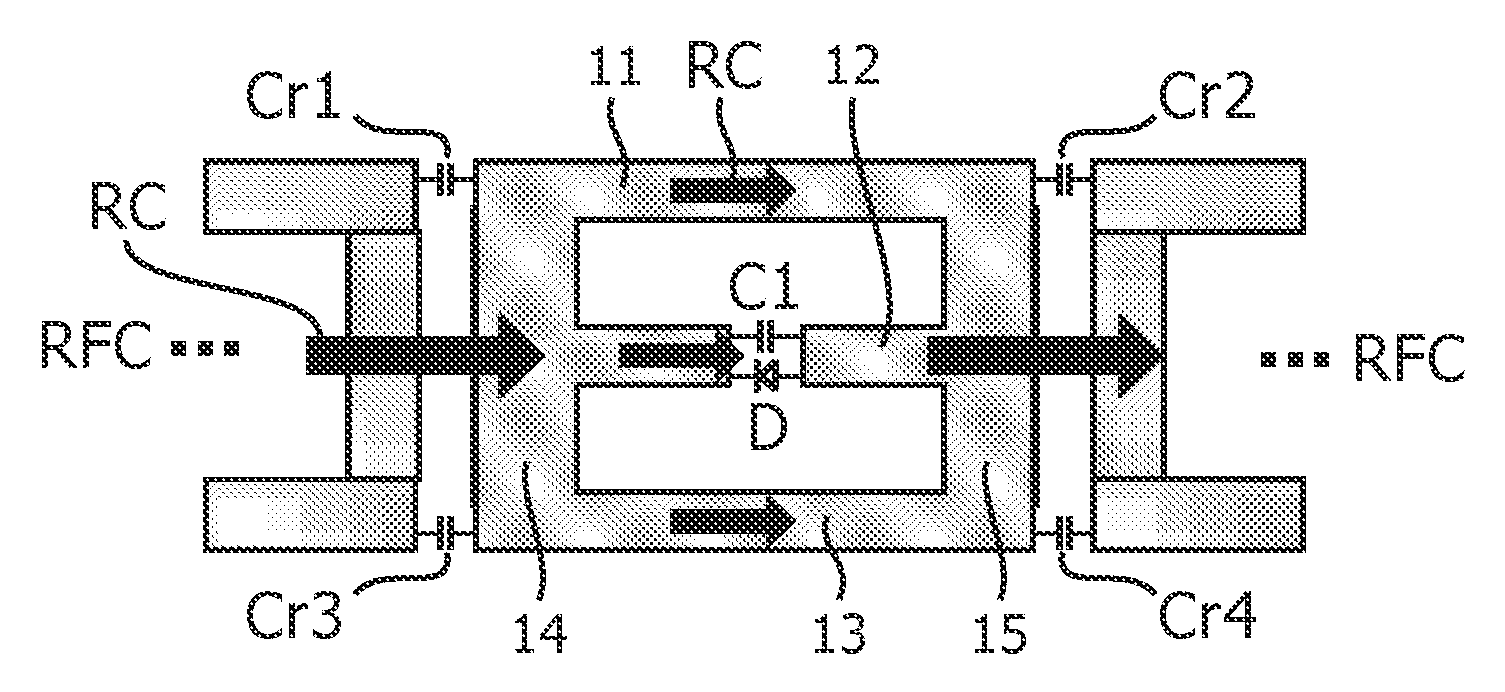
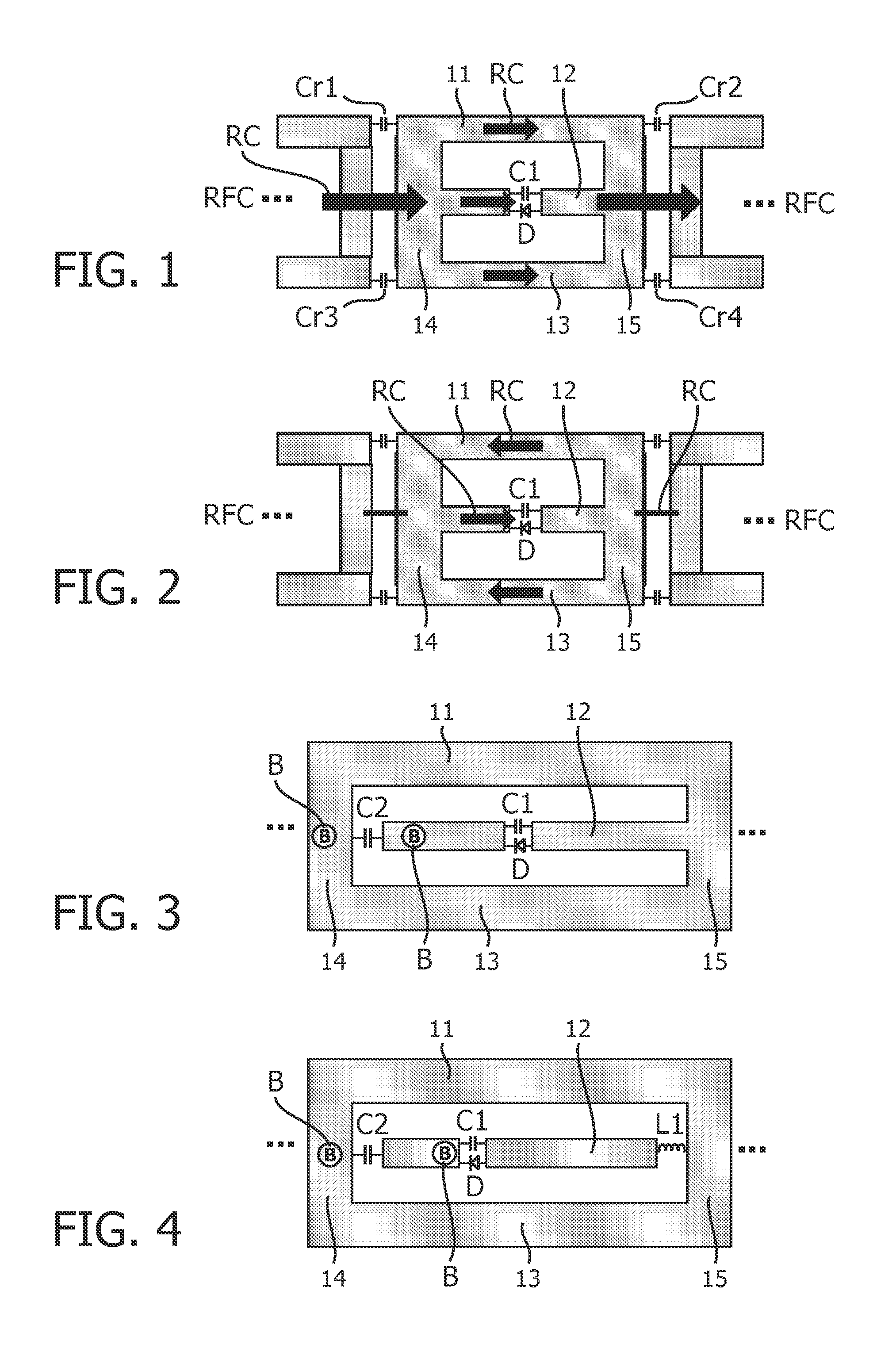
[0062]FIGS. 1 and 2 show a general structure of a trap circuit according to the invention in the form of a first embodiment, being a part of a resonant conductor structure of an RF antenna or coil which is denoted by “RFC” in these Figures. The trap circuit is serially coupled into the resonant conductor structure of the RF antenna or coil RFC preferably by means of capacitors Cr1, Cr2, Cr3, Cr4 which are preferably provided also for tuning the resonance frequency of the RF antenna or coil for RF / MR signal transmission and / or reception as generally known.
[0063]The trap circuit preferably comprises a first, a second and a third conductor 11, 12, 13 which are connected in parallel by means of a fourth and a fifth conductor 14, 15, so that two conductor loops are formed. As mentioned above, also more than three conductors can be connected in parallel or in another way so that more than two conductor loops having the same or different dimensions are formed. This applies for all embodime...
second embodiment
[0074]More in detail, FIG. 3 shows a trap circuit, again comprising a first, a second and a third conductor 11, 12, 13, connected in parallel to each other by means of a fourth and a fifth conductor 14, 15, wherein the second or middle conductor 12 comprises in series the parallel connection of the diode D and the first capacitor C1 as explained above with reference to FIGS. 1 and 2.
[0075]Additionally, FIG. 3 shows a second capacitor C2 in the form of a DC blocking capacitor which connects a first end of the second conductor 12 with the fourth conductor 14 (or is serially connected into a portion of the second conductor 12 between the diode D and this first end of the second conductor 12, which is electrically the same). Further, at both sides of the DC blocking capacitor C2, connecting terminals B are provided for applying the DC bias voltage or current for the diode D. Usually, the capacitance of such a DC blocking capacitor is chosen such (especially large enough) that the resona...
sixth embodiment
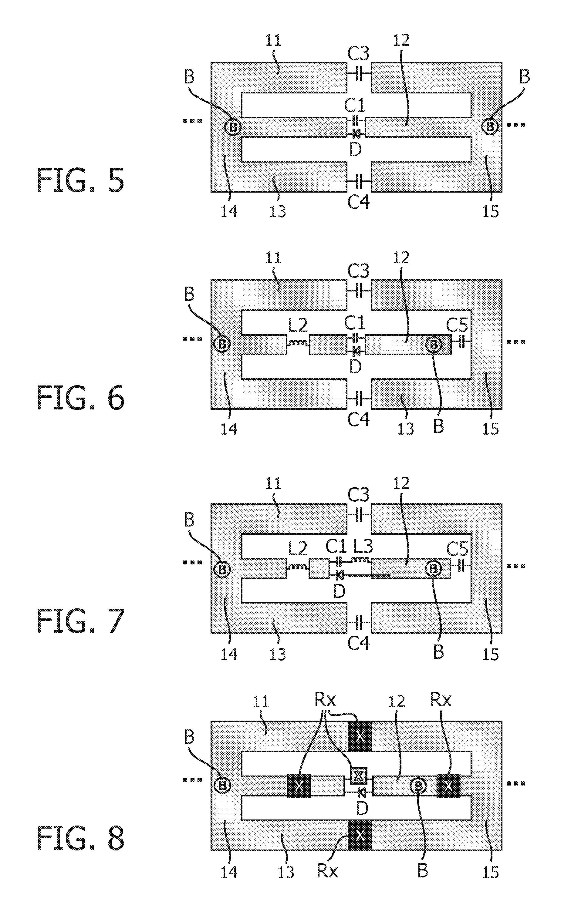
[0082]FIG. 7 shows a trap circuit according to the invention. In comparison to the embodiments as shown in FIGS. 1 to 6 in which the reactive element which is connected in parallel to the diode D is the first capacitor C1 only, in the embodiment according to FIG. 7, this reactive element is a serial connection of the first capacitor C1 and a third inductor L3. The third inductor L3 is provided together with the other reactive elements C1, C3, C4, C5 and L2 (which are connected into the trap circuit as explained above with reference to FIGS. 3 to 6) such that when the diode D is in the non conducting state, a trap resonance can be excited, which effectively traps or blocks the resonant current of the RF antenna and by this detunes this RF antenna or coil as explained above.
[0083]FIG. 8 shows a generalized trap circuit according to the invention in which the various possible positions of reactive elements Rx which are serially connected into at least one of the first, the second and t...
PUM
 Abstract
Description
Claims
Application Information


