Electronic component and method for manufacturing electronic component

a technology of electronic components and manufacturing methods, applied in the field of electronic components, can solve the problems of affecting etchant can damage the capacitor element itself, and etchant can significantly affect the capacitor element, so as to prevent the degradation of the characteristics of the electronic component, reduce the size of the portion, and ensure the effect of corrosion resistan

Inactive Publication Date: 2013-08-15
TDK CORPARATION
View PDF10 Cites 35 Cited by
  • Summary
  • Abstract
  • Description
  • Claims
  • Application Information

AI Technical Summary

Benefits of technology

[0017]In the present invention, the thick film electrode is formed on the end face of the element body. The electronic component, in general, has an internal conductor arranged in the element body and exposed in the end face, and the internal conductor is connected to the thick film electrode. For this reason, the electrical connection between the internal conductor and the thick film electrode and the adherence strength of the thick film electrode to the element body are ensured at a necessary and sufficient level. Through the step of forming the electroconductive thin film, the step of forming the resist layer, the step of removing the electroconductive thin film not covered by the resist layer, and the step of peeling off the resist layer, the electroconductive thin film is formed so as to cover the thick film electrode and the partial region of the principal face and/or the partial region of the side face and the electroconductive thin film function as a thin film electrode. The thick film electrode is formed substantially on the end face and the electroconductive thin film is formed on the partial region of the principal face and/or on the partial region of the side face adjacent to the end face. This configuration drastically reduces the size of the portion of the external electrode located on the principal face and/or the side face of the element body. As a consequence, the electronic component can be realized in a compact size. The thick film electrode and the electroconductive thin film formed thereon are located on the end face of the element body, and in formation of the plated layer, they prevent the plating solution from infiltrating through the end face into the element body. Therefore, this configuration can prevent the degradation o

Problems solved by technology

If the electroconductive coating is not appropriately formed on the end face where the internal electrodes are exposed, a plating solution will infiltrate through the end face into the capacitor element during formation of a plated layer thereon, and the infiltrating plating solution will degrade characteristics of the electronic component.
In the wet etching process, the etchant can damage the capacitor element

Method used


Image

  • Electronic component and method for manufacturing electronic component
  • Electronic component and method for manufacturing electronic component
  • Electronic component and method for manufacturing electronic component

Examples


Embodiment Construction

[0028]The preferred embodiments of the present invention will be described below in detail with reference to the accompanying drawings. In the description, the same elements or elements with the same functionality will be denoted by the same reference signs, without redundant description.

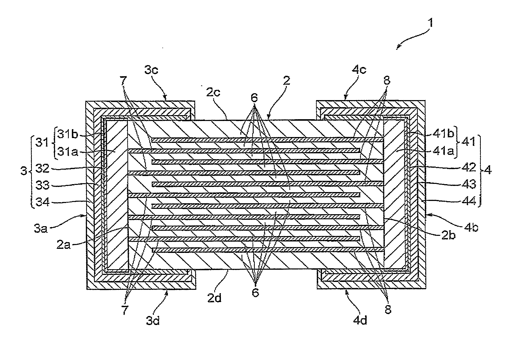
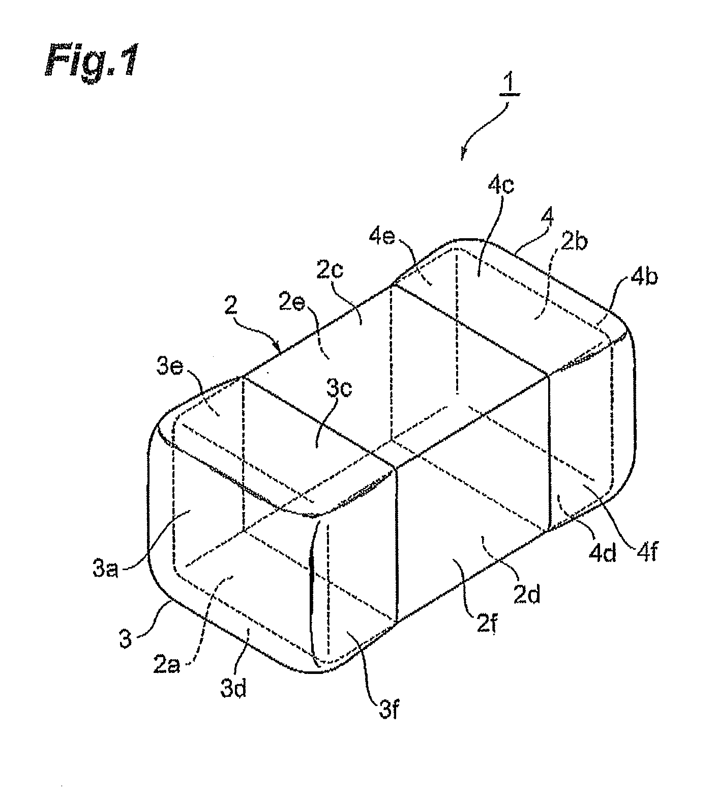
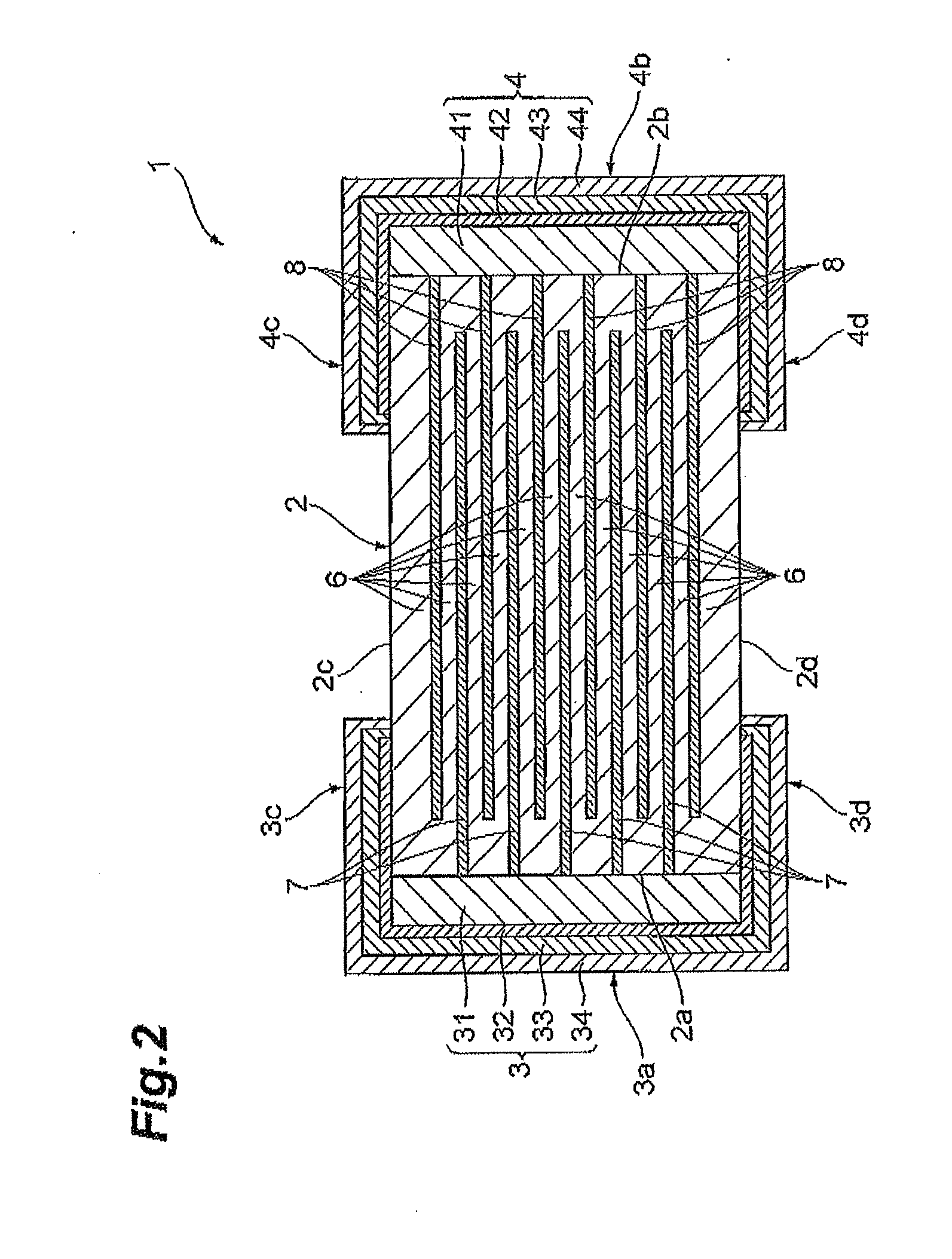
[0029]A configuration of an electronic component 1 according to an embodiment of the present invention will be described with reference to FIGS. 1 and 2. FIG. 1 is a perspective view showing the electronic component of the present embodiment. FIG. 2 is a drawing for explaining the sectional configuration of the electronic component of the present embodiment.

[0030]The electronic component 1 is, for example, an electronic component such as a multilayer ceramic capacitor and is provided with an element body 2 and a plurality of external electrodes 3, 4. The element body 2 is constructed in a nearly rectangular parallelepiped shape by laminating and integrating a plurality of ceramic green sheets. The e...


PUM

PropertyMeasurementUnit
Thicknessaaaaaaaaaa
Electrical conductoraaaaaaaaaa

Abstract

An electronic component has an element body and an external electrode arranged on the element body. The element body has a pair of end faces opposed to each other, a pair of principal faces opposed to each other, and a pair of side faces opposed to each other. The external electrode is formed so as to cover the end face and a partial region of the principal face and/or a partial region of the side face. The external electrode has a thick film electrode, a thin film electrode, and a plated layer. The thick film electrode is formed on the end face. The thin film electrode is formed so as to cover the thick film electrode and the partial region of the principal face and/or the partial region of the side face. The plated layer is formed outside the thin film electrode and contains Sn or an Sn alloy.

Description

BACKGROUND OF THE INVENTION[0001]1. Field of the Invention[0002]The present invention relates to an electronic component and a method for manufacturing the electronic component.[0003]2. Related Background Art[0004]As a method of forming an external electrode of an electronic component, there is a known method including a step of forming an electroconductive coating on a capacitor element by a plasma sputtering process, a step of forming a protective coating of a resist material on a terminal portion of the capacitor element with the electroconductive coating thereon, a step of removing the electroconductive coating from the region other than the terminal portion by etching, and, thereafter, a step of removing the resist (e.g., of Japanese Patent Application Laid-open No. H01-152712). Another known external electrode forming method is one including applying an electroconductive paste onto a main body of the electronic component and sintering it to form a first electrode layer, and th...

Claims


Application Information

Patent Timeline
IPC IPC(8): H01G13/06H01G4/008
CPCH01G13/06H01G4/008H01G4/2325H01G4/12H01G4/30
Inventor SHIRAKAWA, YUKIHIKOTAKAMATSU, YASUHITOHIROSE, OSAMUNAKAMURA, KAZUHIROHIROTA, DAISUKE
Owner TDK CORPARATION
Why Eureka
Try Eureka