High voltage semiconductor element and operating method thereof

a high-voltage semiconductor and operating method technology, applied in the field of semiconductor elements and an operating method thereof, can solve the problems of physical destruction at the surface junction region, the risk of damage of protected devices or internal circuits, and the difficulty of on-chip electro-static discharge protection design, etc., and achieve the effect of not increasing the volume of high-voltage semiconductor elements

Active Publication Date: 2013-08-22
MACRONIX INT CO LTD
View PDF2 Cites 9 Cited by
  • Summary
  • Abstract
  • Description
  • Claims
  • Application Information

AI Technical Summary

Benefits of technology

[0012]The invention is directed to a high voltage semiconductor element and an operating method thereof. A high voltage metal-oxide-semiconductor transistor (HVMOS) and an electro-static discharge bipolar transistor (ESD BJT) are integrated into one element, such that it can prevent from a latch-up, any mask or any manufacturing step will not be added and the volume of the high voltage semiconductor element will not be increased too much.

Problems solved by technology

An operating voltage of a semiconductor element for the BCD manufacturing technology has been higher and higher, such that an on-chip electro-static discharge (ESD) protection design becomes a challenging task.
High voltage current and high electric field will cause a physical destruction at a surface junction region.
Therefore, it is a challenge to get a better ESD protection structure.
Therefore, a protected device or an internal circuit usually has risks of damages, before the high voltage semiconductor element turns on an ESD protection during the electro-static event.
There is a possibility that the high voltage semiconductor element is triggered by an unwanted noise, a power-on peak voltage or a serge voltage and a latch-up may occur during a normal operation.

Method used


Image

  • High voltage semiconductor element and operating method thereof
  • High voltage semiconductor element and operating method thereof
  • High voltage semiconductor element and operating method thereof

Examples


first embodiment

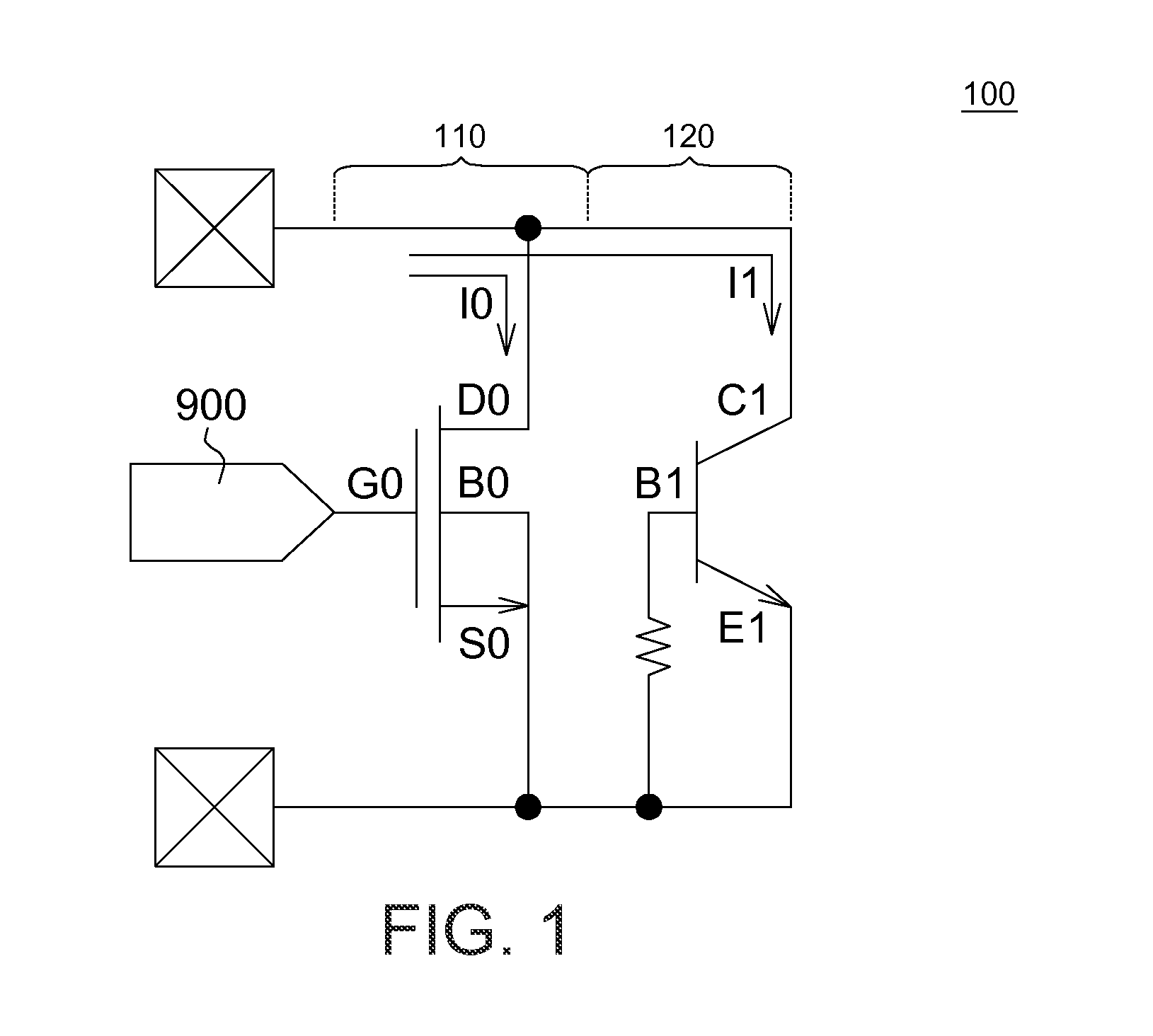
[0021]Referring to FIG. 1, a circuit diagram of a high voltage semiconductor element 100 according to a first embodiment is shown. The high voltage semiconductor element 100 has a high voltage metal-oxide-semiconductor transistor (HVMOS) 110 and a NPN type electro-static discharge bipolar transistor (ESD BJT) 120. The HVMOS 110 is used for switching a high voltage current. The HVMOS 110 has a drain D0, a source S0, a gate G0 and a base B0. The gate G0 is electronically connected to an internal circuit 900. When an inputting voltage of the gate G0 is higher than a trigger voltage, the HVMOS is switched on.

[0022]The NPN type ESD BJT 120 is used for receiving an unnecessary electro-static current for preventing the HVMOS 110 from any damage caused by the electro-static current. The NPN type ESD BJT 120 has a collector C1, an emitter E1 and a base B1. The collector C1 is electronically connected to the drain D0. The emitter E1 is electronically connected to the source S0.

[0023]In the pr...

second embodiment

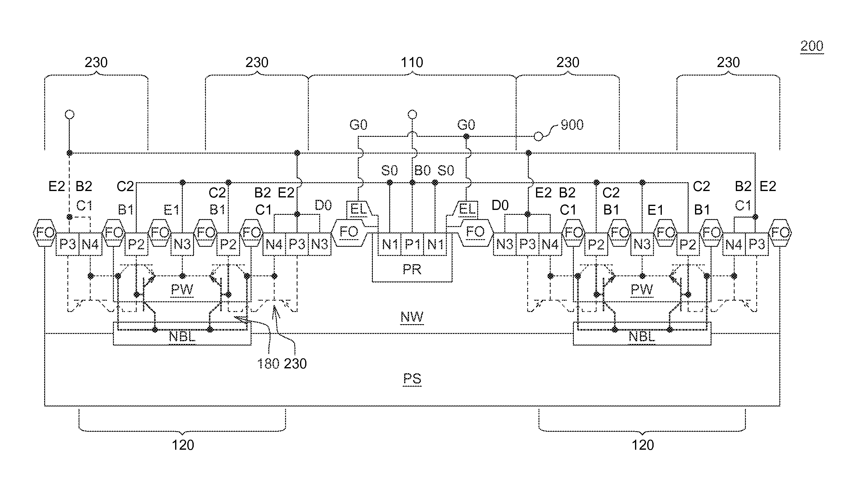
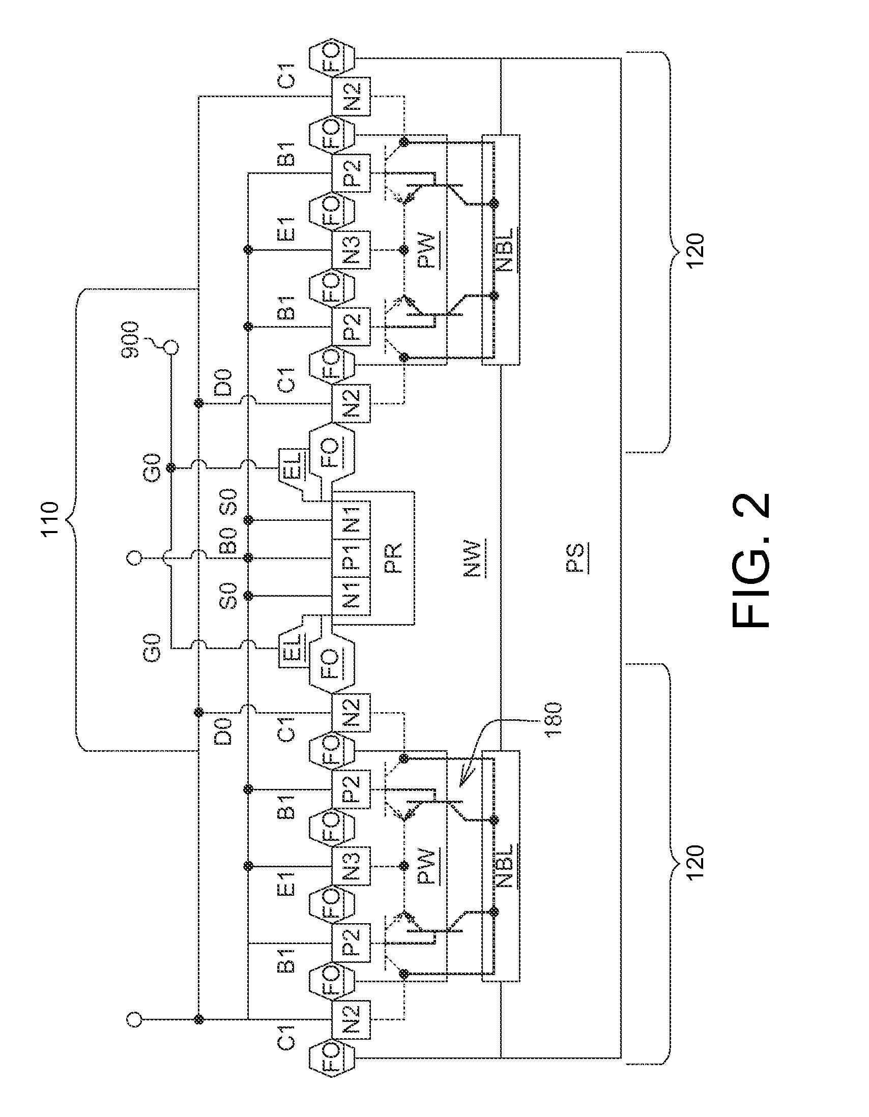
[0033]Please refer to FIG. 3, which shows a circuit diagram of a high voltage semiconductor element according to a second embodiment. The high voltage semiconductor element 200 and an operating method thereof of the present embodiment are different from the high voltage semiconductor element 100 and the operating method thereof of the first embodiment in that the high voltage semiconductor element 200 further comprises a PNP type ESD BJT 230, and the similarities are not repeated here.

[0034]As shown as FIG. 3, the PNP type ESD BJT 230 and the NPN type ESD BJT 120 are connected in parallel. The PNP type ESD BJT 230 has a collector C2, an emitter E2 and a base B2. The emitter E2 is electronically connected to the drain D0 and the collector C1. The collector C2 is electronically connected to the source S0 and the emitter E1.

[0035]In the present embodiment, the HVMOS 110, the NPN type ESD BJT 120 and the PNP type ESD BJT 230 can be integrated in one element by the BCD manufacturing tech...


PUM


Abstract

A high voltage semiconductor element and an operating method thereof are provided. The high voltage semiconductor element comprises a high voltage metal-oxide-semiconductor transistor (HVMOS) and a NPN type electro-static discharge bipolar transistor (ESD BJT). The HVMOS has a drain and a source. The NPN type ESD BJT has a first collector and a first emitter. The first collector is electronically connected to the drain, and the first emitter is electronically connected to the source.

Description

BACKGROUND OF THE INVENTION[0001]1. Field of the Invention[0002]The invention relates in general to a semiconductor element and an operating method thereof, and more particularly to a high voltage semiconductor element and an operating method thereof.[0003]2. Description of the Related Art[0004]With the development of semiconductor technology, a bipolar COMS DMOS (BCD) manufacturing technology has been widely used for a high voltage semiconductor element. An operating voltage of a semiconductor element for the BCD manufacturing technology has been higher and higher, such that an on-chip electro-static discharge (ESD) protection design becomes a challenging task.[0005]A high voltage semiconductor element usually has low on-state resistance (Rdson), so an electro-static current is likely to concentrate in a surface or an edge of a drain during an electro-static event. High voltage current and high electric field will cause a physical destruction at a surface junction region.[0006]Base...

Claims


Application Information

Patent Timeline
Patent Type & Authority Applications(United States)
IPC IPC(8): H03K17/06H01L29/10
CPCH03K17/127H01L27/0259H03K17/567
Inventor CHEN, HSIN-LIANGTUNG, WEN-CHING
Owner MACRONIX INT CO LTD
Why Eureka
Try Eureka