Flowable silicon-carbon-nitrogen layers for semiconductor processing

a technology of silicon carbon-nitrogen and flowable silicon, which is applied in the direction of coating, chemical vapor deposition coating, metallic material coating process, etc., can solve the problems of voids or seams, difficult to fill gaps without dielectric materials, and conventional chemical vapor deposition techniques that experience an overgrowth of materials, etc., to reduce the number of c—h bonds, increase the rate of film aging and contamination, and increase the wet-etch-rate-ratio

Inactive Publication Date: 2013-08-22
APPLIED MATERIALS INC
View PDF7 Cites 380 Cited by
  • Summary
  • Abstract
  • Description
  • Claims
  • Application Information

AI Technical Summary

Benefits of technology

[0007]The initial deposition of the flowable Si—C—N may include significant numbers of Si—H and C—H bonds. These bonds are reactive with the moisture and oxygen in air, as well as a variety of etchants which contributes to an increased rate of film aging and contamination, and higher wet-etch-rate-ratios (WERRs) for the etchants. Following deposition, the Si—C—N film may be cured to reduce the number of Si—H bonds while also increasing the number Si—Si, Si—C, and / or Si—N bonds in the final film. The curing may also reduce the number of C—H bonds and increases the number of C—N and / or C—C bonds in the final film. Curing techniques include exposing the flowable Si—C—N film to a plasma, such as an inductively coupled plasma (e.g., an HDP-CVD plasma) or a capacitively-coupled plasma (e.g., a PE-CVD plasma). In some embodiments, the deposition chamber may be equipped with an in-situ plasma generating system to perform the plasma treatment following the deposition without removing the substrate from the chamber. Alternately, the substrate may be transferred to a plasma treatment unit in the same fabrication system without breaking vacuum and / or being removed from system. This allows the curing step to occur before the initially deposited Si—C—N film has been exposed to moisture and oxygen from the air.
[0008]The final Si—C—N film may exhibit increased etch resistance to both conventional oxide and nitride dielectric etchants. For example, the Si—C—N film may have better etch resistance to a dilute hydrofluoric acid solution (DHF) than a silicon oxide film, and also have better etch resistance to a hot phosphoric acid solution than a silicon nitride film. The increased etch resistance to both conventional oxide and nitride etchants allows these Si—C—N films to remain intact during process routines that expose the substrate to both types of etchants.

Problems solved by technology

As the dimensions continue to get smaller, new challenges arise for seemingly mundane process steps like filling a gap between circuit elements with a dielectric material that acts as electrical insulation.
As the width between the elements continues to shrink, the gap between them often gets taller and narrower, making the gap difficult to fill without the dielectric material getting stuck to create voids and weak seams.
Conventional chemical vapor deposition (CVD) techniques often experience an overgrowth of material at the top of the gap before it has been completely filled.
This can create a void or seam in the gap where the depositing dielectric material has been prematurely cut off by the overgrowth; a problem sometimes referred to as breadloafing.
While the liquid precursor has fewer breadloafing problems, other problems arise when the precursor material is converted to the dielectric material.
The increased porosity left in the final dielectric material can have the same deleterious effects as the voids and weak seams created by conventional CVD techniques.

Method used


Image

  • Flowable silicon-carbon-nitrogen layers for semiconductor processing
  • Flowable silicon-carbon-nitrogen layers for semiconductor processing
  • Flowable silicon-carbon-nitrogen layers for semiconductor processing

Examples


Embodiment Construction

[0018]Methods are described for applying flowable CVD techniques to the formation of flowable silicon-carbon-nitrogen containing materials. These flowable Si—C—N films may be further treated to form Si—C—N blanket layers, gapfills, and sacrificial barriers (among other elements) useful in the fabrication of integrated circuits.

Exemplary Si—C—N Formation Methods

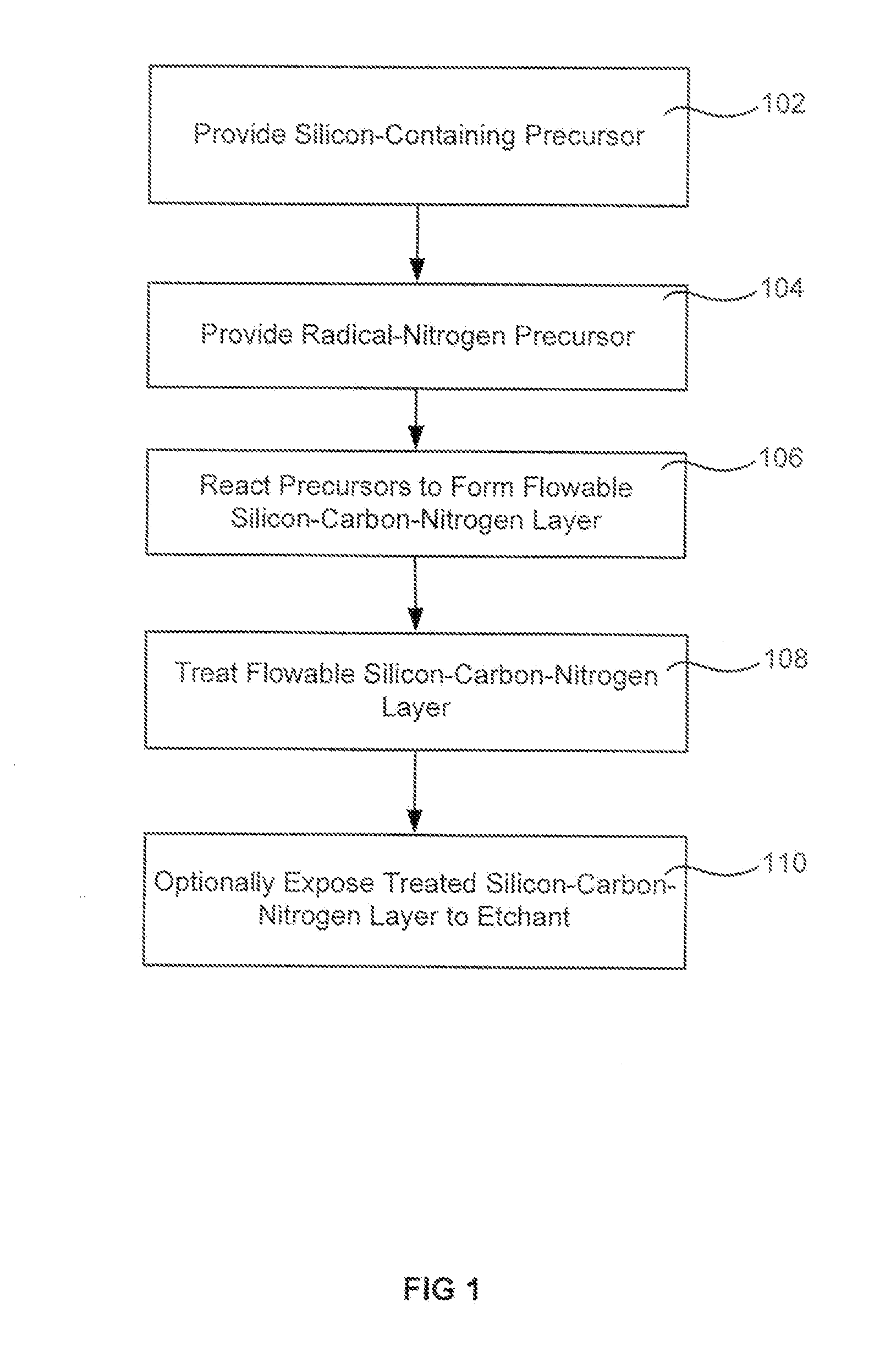
[0019]Referring now to FIG. 1, selected steps in a method of forming a silicon-carbon-nitrogen containing dielectric layer on a substrate. The method may include the step of providing a silicon-containing precursor 102 to a chemical vapor deposition chamber. The silicon-containing precursor may provide the silicon constituent to the deposited Si—C—N film, and may also provide the carbon component. Exemplary silicon-containing precursors include 1,3,5-trisilapentane, 1,4,7-trisilaheptane, disilacyclobutane, trisilacyclohexane, 3-methylsilane, silacyclopentene, silacyclobutane, and trimethylsilylacetylene, among others:

[0020]Add...


PUM

PropertyMeasurementUnit
sizesaaaaaaaaaa
sizesaaaaaaaaaa
sizesaaaaaaaaaa

Abstract

Methods are described for forming a dielectric layer on a semiconductor substrate. The methods may include providing a silicon-containing precursor and an energized nitrogen-containing precursor to a chemical vapor deposition chamber. The silicon-containing precursor and the energized nitrogen-containing precursor may be reacted in the chemical vapor deposition chamber to deposit a flowable silicon-carbon-nitrogen material on the substrate. The methods may further include treating the flowable silicon-carbon-nitrogen material to form the dielectric layer on the semiconductor substrate.

Description

CROSS-REFERENCES TO RELATED APPLICATIONS[0001]This application claims the benefit of U.S. Provisional Application No. 61 / 536,380, filed Sep. 19, 2011, and titled “FLOWABLE SILICON-AND-CARBON-CONTAINING LAYERS FOR SEMICONDUCTOR PROCESSING.” This application also claims the benefit of U.S. Provisional Application No. 61 / 532,708 by Mallick et al. filed Sep. 9, 2011 and titled “FLOWABLE SILICON-CARBON-NITROGEN LAYERS FOR SEMICONDUCTOR PROCESSING.” This application also claims the benefit of U.S. Provisional Application No. 61 / 550,755 by Underwood et al, filed Oct. 24, 2011 and titled “TREATMENTS FOR DECREASING ETCH RATES AFTER FLOWABLE DEPOSITION OF SILICON-CARBON-AND-NITROGEN-CONTAINING LAYERS.” This application also claims the benefit of U.S. Provisional Application No. 61 / 567,738 by Underwood et al, filed Dec. 7, 2011 and titled “DOPING OF DIELECTRIC LAYERS.” Each of the above U.S. Provisional applications is incorporated herein in its entirety for all purposes.BACKGROUND OF THE INVE...

Claims


Application Information

Patent Timeline
Patent Type & Authority Applications(United States)
IPC IPC(8): H01L21/02
CPCH01L21/02167H01L21/02211C23C16/36H01L21/0234H01L21/31111H01L21/02274
Inventor MALLICK, ABHIJIT BASUINGLE, NITIN K.WANG, LINLINUNDERWOOD, BRIAN S.
Owner APPLIED MATERIALS INC
Why Eureka
Try Eureka