Materials and methods for stress reduction in semiconductor wafer passivation layers

Active Publication Date: 2013-09-05
DESIGNER MOLECULES
View PDF86 Cites 51 Cited by
  • Summary
  • Abstract
  • Description
  • Claims
  • Application Information

AI Technical Summary

Benefits of technology

[0015]According to embodiments of the invention, a device is provided, comprising a semiconductor wafer and a passivating layer disposed on the surface of the wafer. According to some embodiments, the passivating layer is comprised of a polyimide polymer having the molecular weight fraction of the combined contents of nitrogen and oxygen that is less than about 20%, such as imide-extended bismaleimides, or graf

Problems solved by technology

This imidization step also requires the evaporation of high boiling, polar aprotic solvents, which can be difficult to drive away as the polyimide is formed.
Moreover, as silicon wafers have become thinner, it has been found that the polyimides used for passivation layers tend to warp the wafer upon thermal cure, resulting in a concave or convex wafer surface.
This phenomenon creates a variety of problems for the semiconductor fabrication and packa

Method used


Image

  • Materials and methods for stress reduction in semiconductor wafer passivation layers
  • Materials and methods for stress reduction in semiconductor wafer passivation layers
  • Materials and methods for stress reduction in semiconductor wafer passivation layers

Examples


example 1

Elongation / Breaking Strength—Dogbone Samples on Instron

[0156]Tensile strength and elongation were measured on an imide-extended bismaleimide resin that had been prepared according to U.S. Pat. No. 7,208,566 in order to demonstrate the mechanical characteristics of compositions of the invention. The resin used in this example was prepared according to Example 5 of that U.S. Pat. No. 7,208,566. The resin had been precipitated into acetone to remove any remaining lower molecular weight residues. In this form (designated as R1130) the approximate molecular weight of the imide extended bismaleimide is around 3,000 Daltons (and is therefore also known as BMI-3000). In this example, two cure conditions were examined: (a) cured via UV exposure only, and (b) UV exposure followed by a thermal post reaction. The UV process parameters were not optimized for intensity, wavelength or protection from O2 inhibition. Specimen dimensions were: 13 mm wide×1.3 mm thick. The photoinitiator (when present...

example 2

Trials Using Toluene as the Image Development Solvent

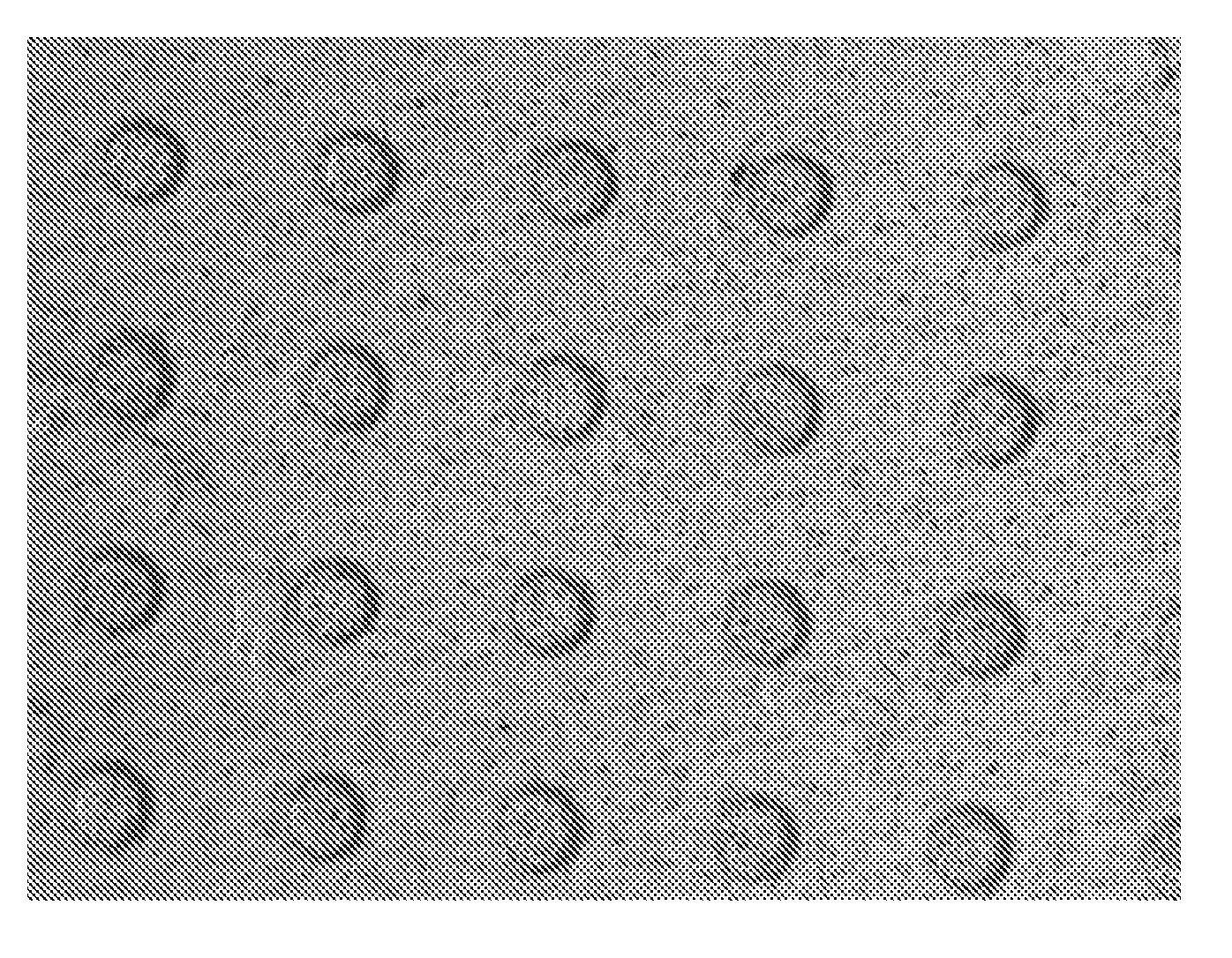
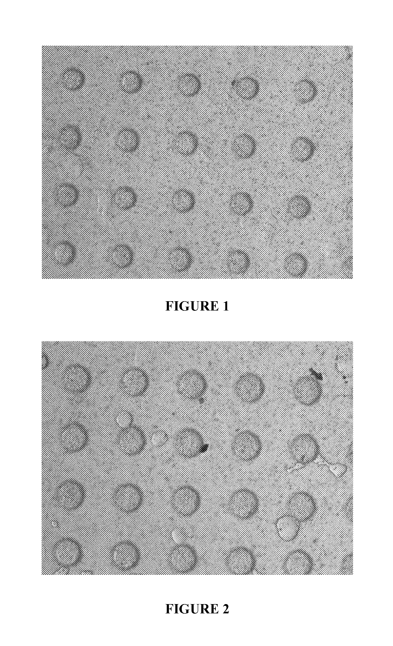
[0158]FIGS. 1-3 show the performance of the materials of the invention in the additional trials that illustrate the applicability of the compositions of the invention to photoimaging applications. Additional trials were performed using the low modulus, imide-extended BMI. Here and below, compound R1184, which was used as such imide-extended BMI, is the compound described in Example 5 of the above-mentioned U.S. Pat. No. 7,208,566, without a subsequent precipitation step, the compound having a molecular weight of about 2,000 Daltons. Compound R1184 was doctor-bladed onto ceramic wafers to form an even coating, followed by UV exposures through masks. The doctor-bladed films were exposed to a broad-spectrum UV light source with the mask interposed between the un-cured film and the light source. The photoimaged films were then developed using a jet of toluene.

[0159]The circular areas in the developed images directly correspond to opaq...

example 3

Trials Using Cyclohexanone as the Image Development Solvent

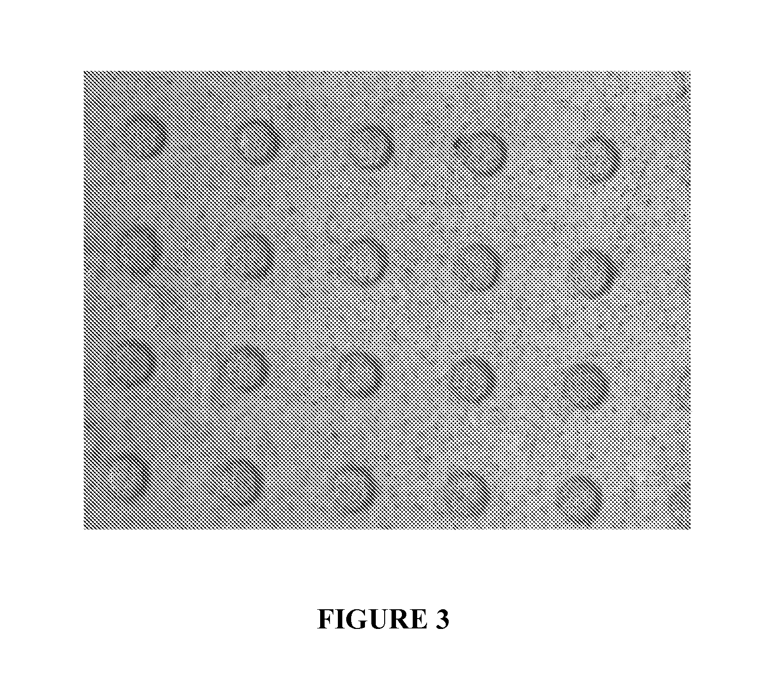
[0162]Cyclohexanone proved to be a suitable solvent for developing photoimaged patterns in compositions of the invention. In this example, the film was spin coated on wafers to achieve 13 um thickness. Coating conditions were: (1) spin 30 seconds at 590 rpm; (2) spin 30 seconds at 1196 rpm; (3) bake 30 minutes at 100° C. (surface is non-tacky). The imaged and developed pattern was characterized using a contact profilometer. In all cases, the replication of mask dimension in the imaged pattern was excellent with very good edge definition. Some of the developing with cyclohexanone was done using s spray device, but flooding followed by a simple rinse with acetone was just as effective. This demonstrates that compositions of the invention are suited to use as photoimagable passivation layers.


PUM

PropertyMeasurementUnit
Temperatureaaaaaaaaaa
Fractionaaaaaaaaaa
Fractionaaaaaaaaaa

Abstract

The present invention provides polyimide polymer materials for passivating semiconductor wafers and methods for fabricating thereof. The present invention further provides a device that includes a semiconductor wafer and a passivating layer disposed on the surface of the wafer, wherein the passivating layer comprises such polyimide polymers.

Description

CROSS REFERENCE TO RELATED APPLICATIONS[0001]This application is claims the benefit of priority under 35 USC §119 of U.S. Provisional Application Ser. No. 61 / 239,758 filed Sep. 3, 2009, the entire disclosure of which is incorporated herein by reference.FIELD OF THE INVENTION[0002]The present invention relates generally to passivating layers for silicon wafers. More particularly, the invention relates to compositions containing low modulus photoimagable polyimides for use as passivating layers.BACKGROUND OF THE INVENTION[0003]Polyimides exhibit an attractive combination of thermal stability (>500° C.), mechanical toughness and chemical resistance, in addition to having excellent dielectric properties. Because of their high degree of ductility and inherently low CTE, polyimides can be readily implemented into a variety of microelectronic applications.[0004]Polyimide films are frequently used as passivation layers for silicon wafers. Polyimide passivation layers are typically 4-6 mi...

Claims


Application Information

Patent Timeline
IPC IPC(8): H01L23/08H01L21/314
CPCH01L21/02282H01L2924/12044C08G73/1014C08G73/106H01L21/02118H01L23/293H01L2924/0002H01L23/08H01L21/314H01L2924/00C08G73/12
Inventor DERSHEM, STEPHEN M.MIZORI, FARHAD G.HUNEKE, JAMES T.
Owner DESIGNER MOLECULES
Why Eureka
Try Eureka