Multilayer ceramic electronic component and method of manufacturing the same

a technology of electronic components and ceramics, applied in the direction of fixed capacitor details, stacked capacitors, fixed capacitors, etc., can solve the problems of increasing the speed of computer central processing units, deteriorating insulation resistance, and deteriorating reliability, so as to reduce the infiltration of foreign substances, improve reliability, and increase the capacitance in a limited volume

Active Publication Date: 2013-09-05
SAMSUNG ELECTRO MECHANICS CO LTD
View PDF6 Cites 16 Cited by
  • Summary
  • Abstract
  • Description
  • Claims
  • Application Information

AI Technical Summary

Benefits of technology

[0019]An aspect of the present invention provides a new method of significantly reducing the infiltration of foreign substances through corner portions of a multilayer ceramic electronic component, to thereby improve reliability and significantly increase the capacitance in a limited volume.

Problems solved by technology

Heat generated in electronic devices is a growing problem, since image display devices have recently become bigger and the speed of computer central processing units (CPUs) has increased.
Therefore, conductive foreign substances such as plating liquid or moisture may infiltrate through the corner portions, which may cause deterioration of insulation resistance and degradation of reliability.

Method used


Image

  • Multilayer ceramic electronic component and method of manufacturing the same
  • Multilayer ceramic electronic component and method of manufacturing the same
  • Multilayer ceramic electronic component and method of manufacturing the same

Examples


Embodiment Construction

[0049]Hereinafter, embodiments of the present invention will be described in detail with reference to the accompanying drawings so that they can be easily practiced by those skilled in the art to which the present invention pertains.

[0050]However, the invention may be embodied in many different forms and should not be construed as being limited to the embodiments set forth herein.

[0051]The embodiments of the present invention are provided so that those skilled in the art may more completely understand the present invention.

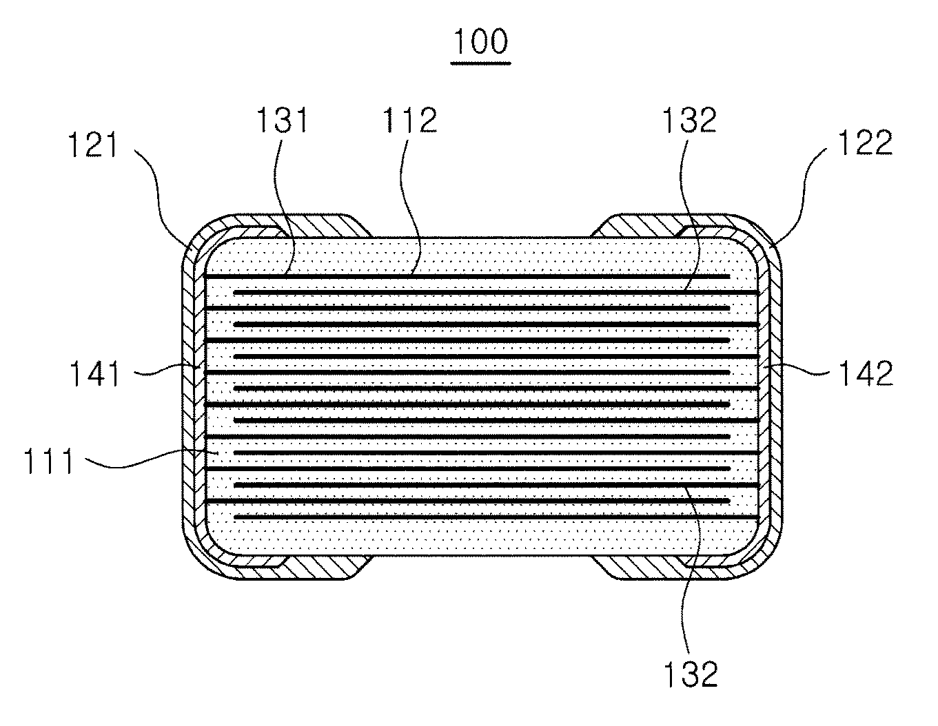
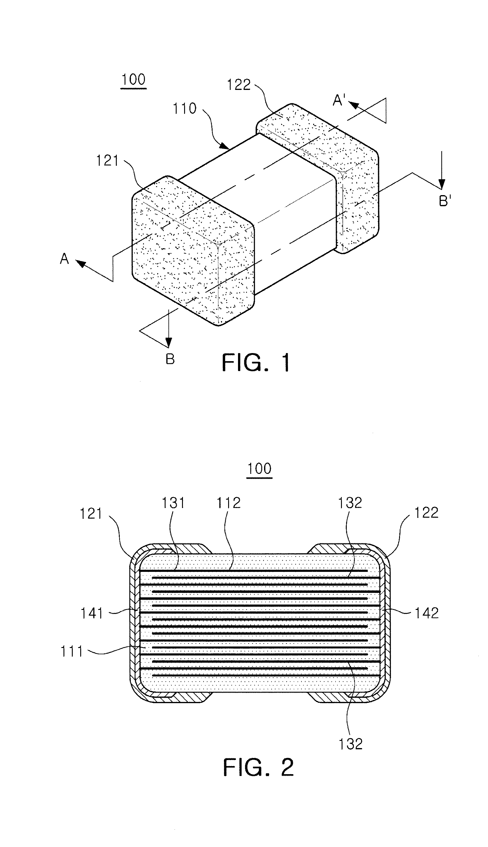
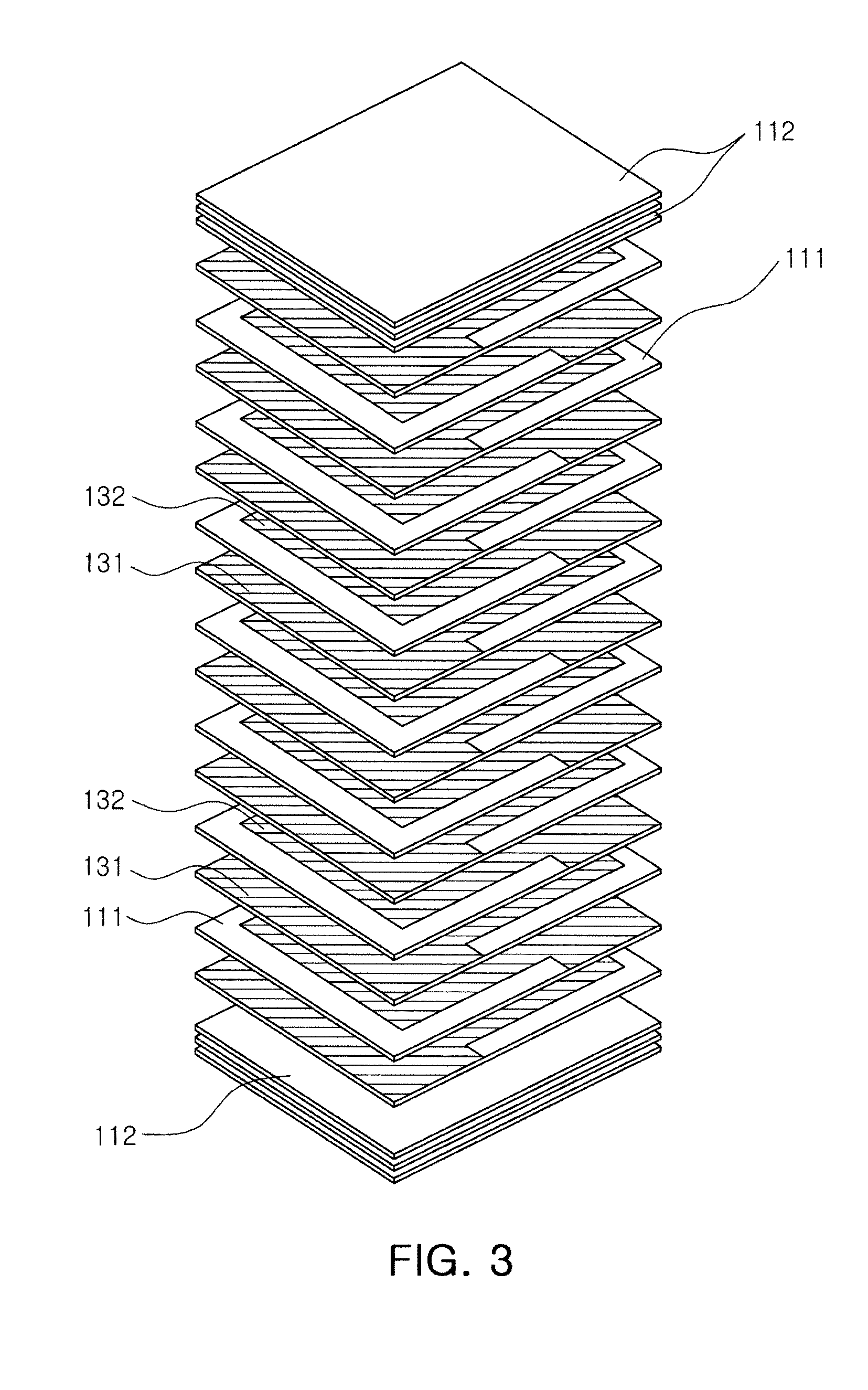
[0052]In the drawings, the shapes and dimensions of components may be exaggerated for clarity, and the same reference numerals will be used throughout to designate the same or like components.

[0053]In addition, like reference numerals denote parts performing similar functions and actions throughout the drawings.

[0054]In addition, unless explicitly described otherwise, “comprising” any components will be understood to imply the inclusion of other components but not...


PUM

PropertyMeasurementUnit
capacitanceaaaaaaaaaa
sizeaaaaaaaaaa
sizeaaaaaaaaaa

Abstract

There is provided a multilayer ceramic electronic component, including: a ceramic sintered body having a plurality of dielectric layers laminated therein; first and second capacitance portions being formed on surfaces of the dielectric layers; first and second lead-out portions being respectively extended from both sides of the first and second capacitance portions to be respectively exposed through both side surfaces of the ceramic sintered body and spaced apart from each other; sealing parts enclosing both end portions and corner portions of the ceramic sintered body; and first and second external electrodes enclosing the sealing parts and formed on both end portions of the ceramic sintered body to be electrically connected to the first and second lead-out portions, respectively.

Description

CROSS-REFERENCE TO RELATED APPLICATIONS[0001]This application claims the priority of Korean Patent Application No. 10-2012-0022376 filed on Mar. 5, 2012, in the Korean Intellectual Property Office, the disclosure of which is incorporated herein by reference.BACKGROUND OF THE INVENTION[0002]1. Field of the Invention[0003]The present invention relates to a multilayer ceramic electronic component and a method of manufacturing the same.[0004]2. Description of the Related Art[0005]As representative electronic components using a ceramic material there are provided a capacitor, an inductor, a piezoelectric element, a varistor, a thermistor and the like.[0006]Among these ceramic electronic components, multilayer ceramic capacitors (MLCCs) have a small size, secure high capacitance, and are easily mountable.[0007]Multilayer ceramic capacitors are chip type condensers that are mounted on circuit boards of various electronic products, such as image display devices, for example, liquid crystal ...

Claims


Application Information

Patent Timeline
Patent Type & Authority Applications(United States)
IPC IPC(8): H01G4/12
CPCH01G4/12H01G4/232H01G4/012H01G4/30H01G4/228H01G4/005
Inventor LEE, CHUNG EUNCHOI, JAE YEOLKIM, DOO YOUNGKIM, WI HEON
Owner SAMSUNG ELECTRO MECHANICS CO LTD
Why Eureka
Try Eureka