Flowable oxide film with tunable wet etch rate

a flowable oxide film and wet etching technology, which is applied in the direction of basic electric elements, semiconductor/solid-state device manufacturing, electric apparatus, etc., can solve the problems of increasing difficulty in void-free filling of narrow width, reducing budget, and increasing difficulty in high aspect ratio (ar) features (e.g., ar>6:1). to achieve the effect of increasing or decreasing wer

Active Publication Date: 2013-09-05
NOVELLUS SYSTEMS
View PDF5 Cites 228 Cited by
  • Summary
  • Abstract
  • Description
  • Claims
  • Application Information

AI Technical Summary

Benefits of technology

[0006]Another aspect relates to tuning the WER of flowable oxide films. According to various embodiments, flowable oxide films can be treated to increase or decrease the WER. In some embodiments, the treatment processes can include exposure to reactive species and / or exposure to electromagnetic radiation. In some embodiments, the treatment processes can be performed after patterning and partial integration
[0007]These and other aspects of the invention are described more fully below with reference to the drawings.

Problems solved by technology

As device geometries shrink and thermal budgets are reduced, void-free filling of narrow width, high aspect ratio (AR) features (e.g., AR>6:1) becomes increasingly difficult due to limitations of existing deposition processes.

Method used


Image

  • Flowable oxide film with tunable wet etch rate
  • Flowable oxide film with tunable wet etch rate
  • Flowable oxide film with tunable wet etch rate

Examples


Embodiment Construction

Introduction

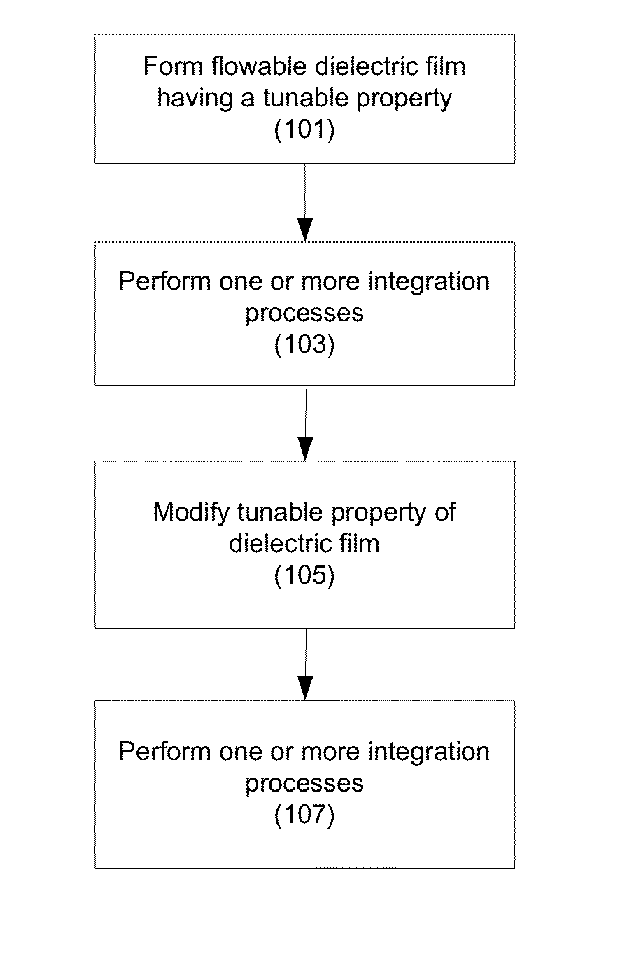
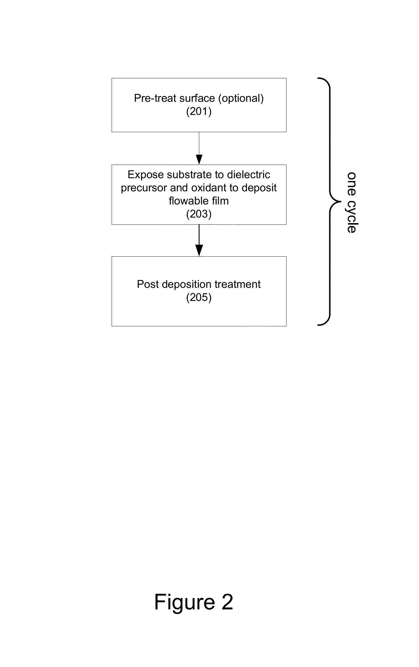
[0023]Aspects of the present invention relate to flowable dielectric films, including the deposition and tuning of flowable dielectric films and related integration schemes. Some embodiments include filling high aspect ratio gaps with insulating material. While the description below refers chiefly to flowable silicon oxide films, the integration schemes described herein may also be used with other types of flowable dielectric films. For example, the dielectric film may be primarily silicon nitride, with Si—N and N—H bonds, primarily silicon oxynitride, primarily silicon carbide or primarily silicon oxycarbide

[0024]Vapor-phase reactants are introduced to a deposition chamber to deposit the flowable dielectric films. As-deposited, the flowable dielectric films generally have flow characteristics that can provide consistent fill of a gap, though according to various embodiments, they can be used to deposit overburden layers, blanket layers, and other non-gap fill processes ...


PUM

PropertyMeasurementUnit
wet etch rateaaaaaaaaaa
chamber pressureaaaaaaaaaa

Abstract

Provided herein are integration-compatible dielectric films and methods of depositing and modifying them. According to various embodiments, the methods can include deposition of flowable dielectric films targeting specific film properties and/or modification of those properties with an integration-compatible treatment process. In certain embodiments, methods of depositing and modifying flowable dielectric films having tunable wet etch rates and other properties are provided. Wet etch rates can be tuned during integration through am integration-compatible treatment process. Examples of treatment processes include plasma exposure and ultraviolet radiation exposure.

Description

CROSS-REFERENCE TO RELATED APPLICATION[0001]This application is claim benefit under 35 USC §119(e) to U.S. Patent Provisional Patent Application No. 61 / 606,876, filed Mar. 5, 2012, which is incorporated by reference herein.BACKGROUND OF THE INVENTION[0002]It is often necessary in semiconductor processing to fill high aspect ratio gaps with insulating material. This is the case for shallow trench isolation (STI), inter-metal dielectric (IMD) layers, inter-layer dielectric (ILD) layers, pre-metal dielectric (PMD) layers, passivation layers, etc. As device geometries shrink and thermal budgets are reduced, void-free filling of narrow width, high aspect ratio (AR) features (e.g., AR>6:1) becomes increasingly difficult due to limitations of existing deposition processes.SUMMARY OF THE INVENTION[0003]Provided herein are integration-compatible dielectric films and methods of depositing and modifying them. According to various embodiments, the methods can include deposition of flowable d...

Claims


Application Information

Patent Timeline
Patent Type & Authority Applications(United States)
IPC IPC(8): H01L21/268
CPCH01L21/02126H01L21/0214H01L21/02164H01L21/02167H01L21/0217H01L21/02271H01L21/02343H01L21/02299H01L21/02337H01L21/0234H01L21/02348H01L21/31111H01L21/02274H01L21/30604
Inventor DRAEGER, NERISSASHANNON, KARENAVAN SCHRAVENDIJK, BARTASHTIANI, KAIHAN
Owner NOVELLUS SYSTEMS
Why Eureka
Try Eureka