

Current-mode CMOS logarithmic function circuit
- Summary
- Abstract
- Description
- Claims
- Application Information
AI Technical Summary
Benefits of technology
Problems solved by technology
Method used
Image

Examples
Embodiment Construction
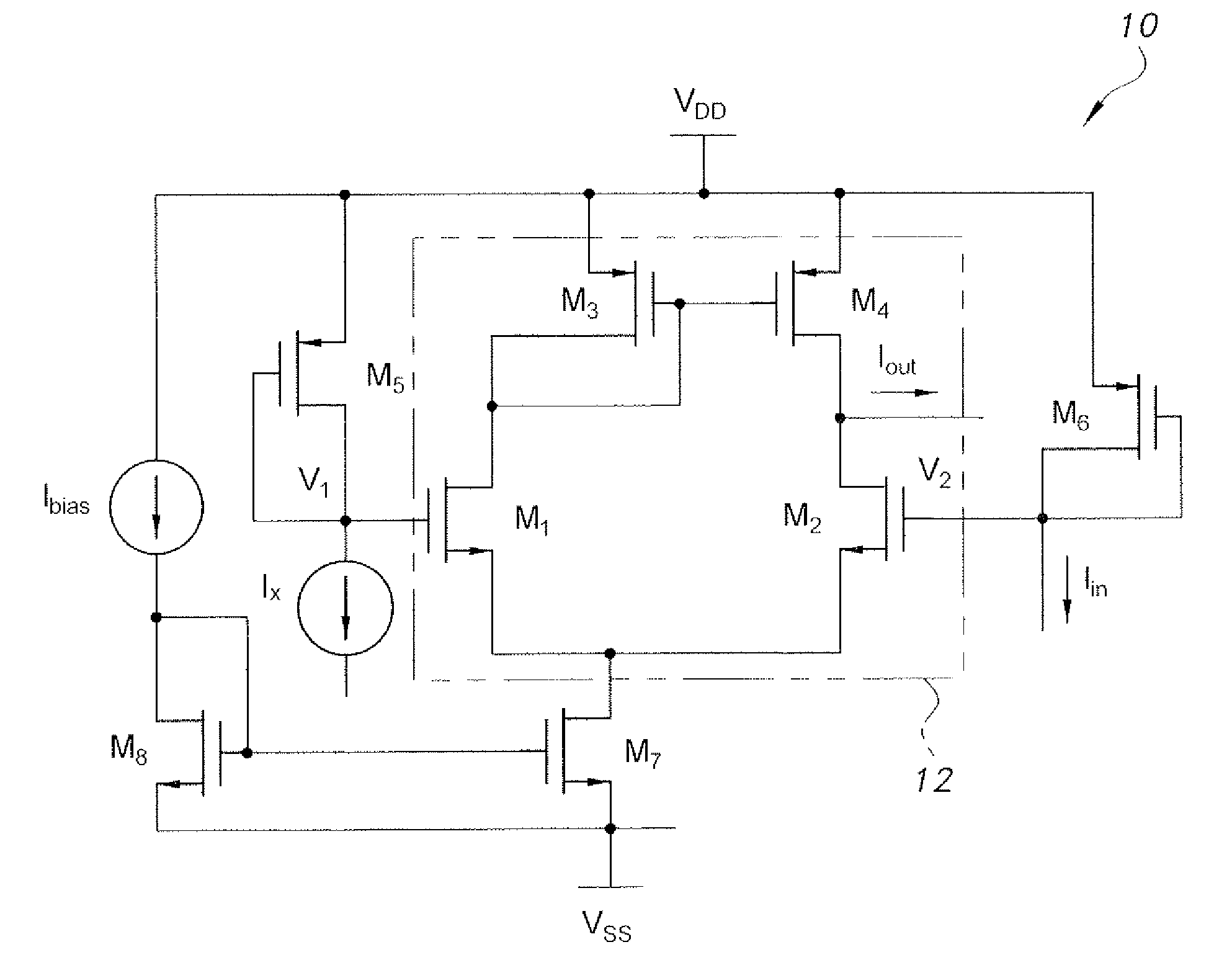
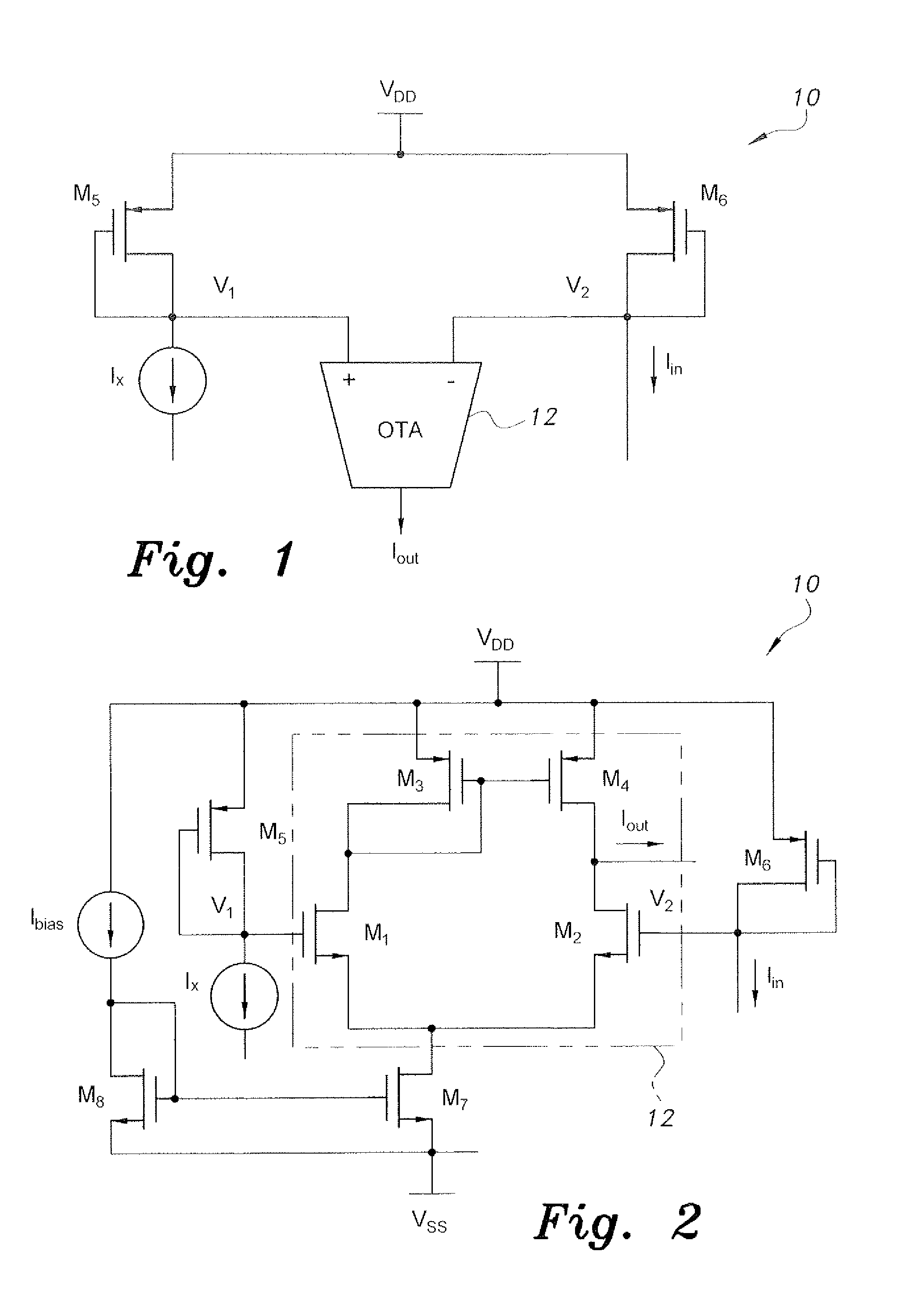
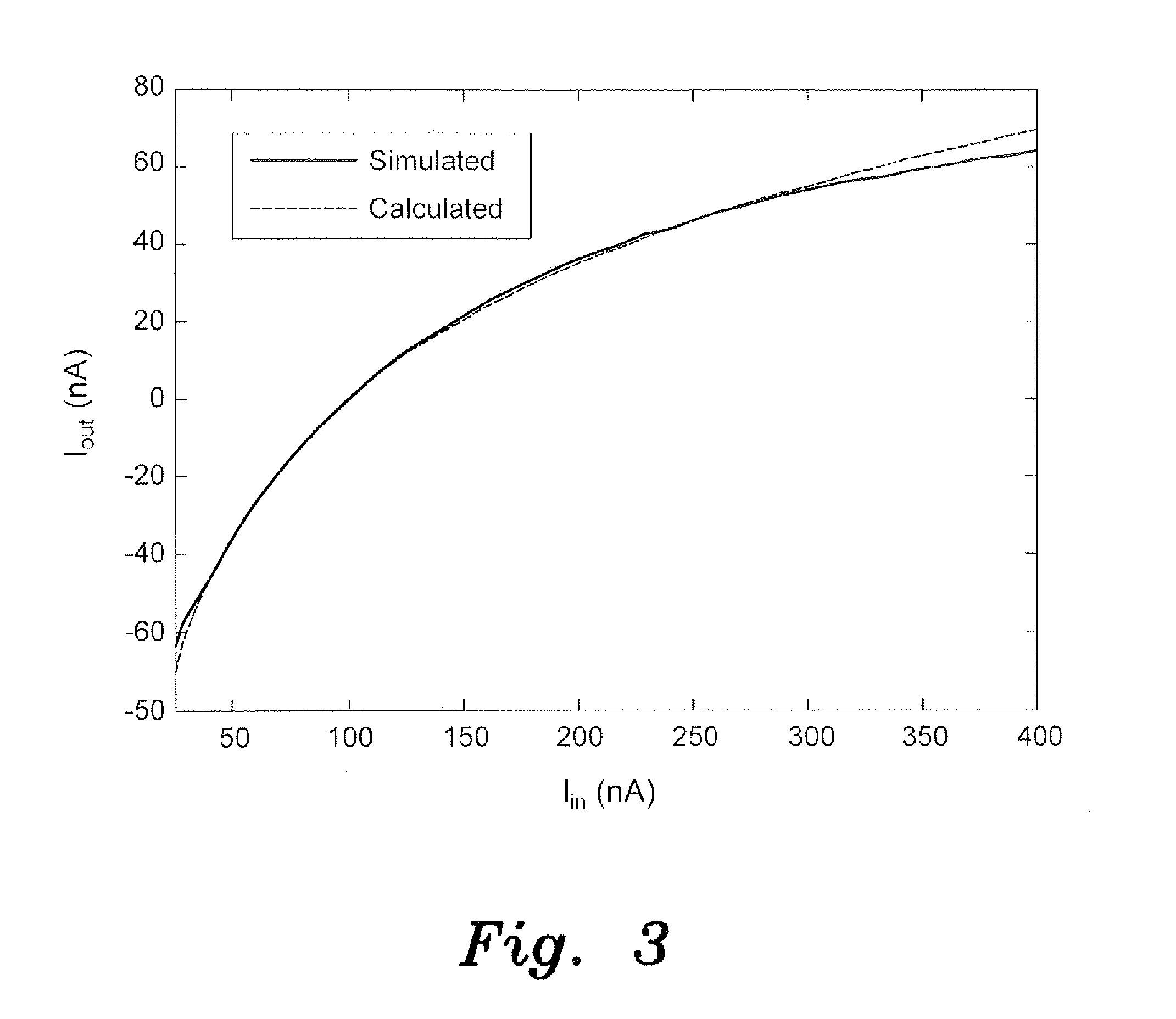
[0012]The current-mode CMOS logarithmic function circuit provides an ultra-low power circuit that produces an output current proportional to the logarithm of the input current. An OTA (operational transconductance amplifier) in combination with two PMOS transistors provides a high dynamic range, controllable amplitude, high accuracy and insensitivity to temperature variation.
[0013]Although theoretically or ideally there should be no current between the drain and source of a MOSFET when the transistor is turned off (the gate-to-source voltage is less than the threshold voltage of the device), in practice there is a weak inversion current that varies exponentially with the gate-to-source bias voltage. This is referred to herein as operation in the weak inversion mode. The current-mode CMOS logarithmic function circuit makes use of this phenomenon to produce an output current proportional to the logarithm (natural logarithm) of the input current.
[0014]The PMOS transistors M5 and M6 are...
PUM
 Abstract
Description
Claims
Application Information