Protective semiconductor device for secondary cell

Inactive Publication Date: 2013-09-19
RICOH ELECTRONIC DEVICES CO LTD
View PDF2 Cites 10 Cited by
  • Summary
  • Abstract
  • Description
  • Claims
  • Application Information

AI Technical Summary

Benefits of technology

[0009]An object of the present invention is to provide a protective semiconductor device which detects an occurrence of a disconnection reliably if a part of the connection between the secondary cells and the protective semiconductor device is disconnected.
[0010]To accomplish the above object, a protective semiconductor device according to one embodiment of the present invention is a protective semiconductor device capable of detecting a voltage state of a plurality of secondary cells connected in series, comprising connecting terminals which are connectable to an electrode of each secondary cell, first resistances detecting the voltage of each of secondary cells which are arranged corresponding to each secondary cell and connected between the terminals corresponding to each electrode of a high-pressure side and low-pressure side, comparators which are arranged corresponding to each secondary cell and capable of detect

Problems solved by technology

However, in conventional protective semiconductor devices which protect the plurality of the secondary cells used by connecting them in series, there is a problem in that the a disconnection cannot be detected when generated at a part of a connection between the secondary ce

Method used


Image

  • Protective semiconductor device for secondary cell
  • Protective semiconductor device for secondary cell
  • Protective semiconductor device for secondary cell

Examples


first embodiment

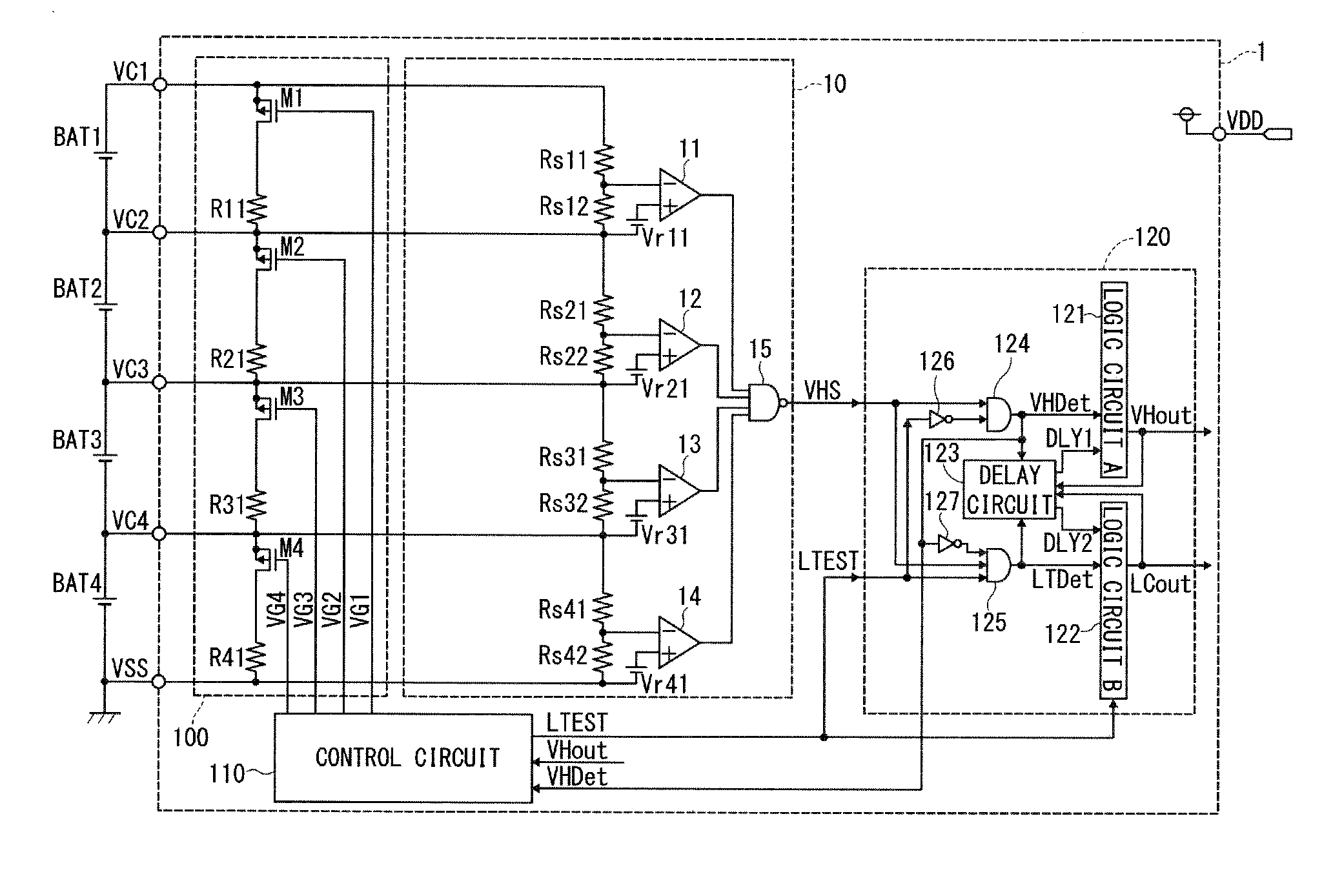
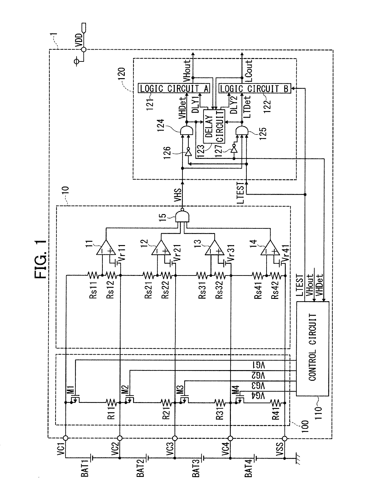
[0027]A first embodiment of the present invention relates to a protective semiconductor device that protects a plurality of secondary cells connected in series and has the following configuration.

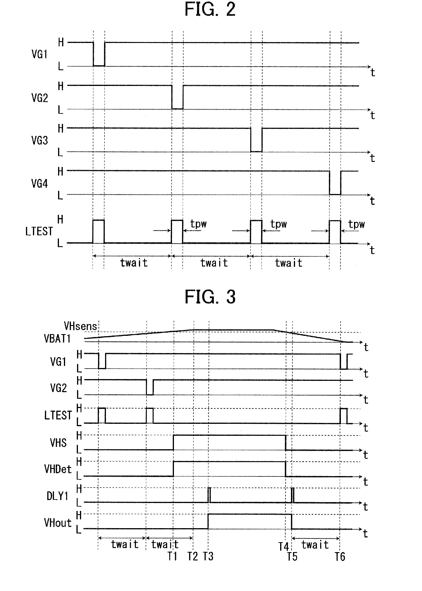
[0028]The protective semiconductor device includes a voltage-sense resistance connected in parallel with the secondary cells to monitor a voltage. A resistance which has a smaller resistance value than that of the voltage-sense resistance is temporarily connected in parallel with the voltage-sense resistance at constant time intervals. If a disconnection between the protective semiconductor device and the secondary sell is not generated, the fluctuation in voltage by the secondary cell is not generated at a connecting terminal of the protective semiconductor device, connected to the secondary sell. On the other hand, if the disconnection between the protective semiconductor device and the secondary sell is generated, voltage fluctuates along with the fluctuation in the resistance value caus...

second embodiment

[0066]The protective semiconductor device according to the first embodiment of the invention has a problem with a false detection of the disconnection between the secondary cells and the protective semiconductor device even though no disconnection has arisen due to the generated voltage at both ends of the resistance forming a low-pass filter during the disconnection test, if the device is connected through a low-pass filter as a measure against noise. Therefore, the protective semiconductor device according to the second embodiment of the invention is characterized by reducing the false detection by the comparators, and the characteristics will be achieved in the following way. By connecting the resistances in series to each voltage-sense resistance of all the secondary cells respectively, while the resistance which has a smaller resistance value is temporarily connected in parallel to the voltage-sense resistance, the inversion level of the comparator connected with the voltage-se...

third embodiment

[0127]The protective semiconductor device according to the second embodiment of the invention sometime does not function normally the operation of the detection of disconnection, if the circuit including the resistance having a lower value is connected to the each secondary cell in parallel in order to even out the voltage of the plurality of the secondary cells. Therefore, the protective semiconductor device according to the third embodiment of the invention enables to function normally the operation of the detection of disconnection by disabling the resistance having the lower value when detecting the disconnection.

3.1 Configuration of the Protective Semiconductor Device

[0128]FIG. 9 is the schematic diagram of the protective semiconductor device 1 according to the third embodiment and the secondary cells. FIG. 10 is the practical schematic diagram of the protective semiconductor device according to the third embodiment and the secondary cells. The protective semiconductor device 1...


PUM


Abstract

Provided is a protective semiconductor device detecting a disconnection reliably with secondary cells including for each cell: cell-connecting terminals; a first resistance detecting the voltage of each cell; a comparator detecting whether or not the voltage of each cell is in the reference voltage range; a series circuit composed of a second resistance and a first switch element, and including a control circuit controlling ON/OFF of the switch element, wherein the first switch element connects the second resistance to the connecting terminals by turning ON, while disconnecting it by turning OFF, the control circuit maintains a disconnection test signal ON, while turning ON the plurality of first switch elements sequentially and detecting the disconnection between the cells and the connecting terminals based on the output signal from the comparator corresponding to the first switch element turned ON.

Description

CROSS-REFERENCE TO RELATED APPLICATION[0001]The present application is based on and claims priority from Japanese Application Number, 2012-062329, filed on Mar. 19, 2012, the disclosure of which is hereby incorporated by reference herein in its entirety.BACKGROUND OF THE INVENTION[0002]1. Field of the Invention[0003]The present invention relates to a protective semiconductor device for a secondary cell.[0004]2. Description of the Related Art[0005]Battery packs, which are easy to handle, have been widely used for mobile electronic devices. Such battery packs are formed of a package in which one or more secondary cells are contained. As the secondary cell, a high-capacity battery such as a lithium-ion battery, a lithium polymer battery, a nickel hydride battery, and so on is used. There is a possibility of evolution of high-temperature heat leading to ignition if an overcharge, an over discharge, an excess current, and so on are generated, since these high-capacity batteries have a hi...

Claims


Application Information

Patent Timeline
IPC IPC(8): H02H3/20
CPCH02H3/207H01M10/482G01R19/16542G01R31/362G01R31/3658H02J7/0016G01R31/396G01R31/3835Y02E60/10
Inventor OSHIMA, MASASHIARAI, KUNIAKIKANNO, JUNICHI
Owner RICOH ELECTRONIC DEVICES CO LTD
Why Eureka
Try Eureka