Calibration Of An Optical Metrology System For Critical Dimension Application Matching

a technology of optical metrology and critical dimension, applied in the direction of testing/monitoring control system, process and machine control, instruments, etc., can solve the problems of loss of consistency among processed semiconductor wafers, difficulty in characterization, and increased difficulty in characterization, so as to enhance application and tool-to-tool matching and high precision

Inactive Publication Date: 2013-09-19
KLA TENCOR TECH CORP
View PDF18 Cites 50 Cited by
  • Summary
  • Abstract
  • Description
  • Claims
  • Application Information

AI Technical Summary

Benefits of technology

[0009]Methods and systems for matching critical dimension measurements at high precision from multiple optical metrology systems are presented. Such systems are employed to measure structural and material characteristics (e.g., material composition, dimensional characteristics of structures and films, etc.) associated with different semiconductor fabrication processes. In one aspect, machine parameter values of a metrology system are calibrated based on critical d...

Problems solved by technology

As devices (e.g., logic and memory devices) move toward smaller nanometer-scale dimensions, characterization becomes more difficult.
Devices incorporating complex three-dimensional geometry and materials with diverse physical properties contribute to characterization difficulty.
If measurement consistency degrades in a manufacturing environment, consistency among processed semiconductor wafers is lost and yield drops to unacceptable levels.
Thus, current methods of tool-to-tool matching do not differentiate betwee...

Method used


Image

  • Calibration Of An Optical Metrology System For Critical Dimension Application Matching
  • Calibration Of An Optical Metrology System For Critical Dimension Application Matching
  • Calibration Of An Optical Metrology System For Critical Dimension Application Matching

Examples


Embodiment Construction

[0016]Reference will now be made in detail to background examples and some embodiments of the invention, examples of which are illustrated in the accompanying drawings.

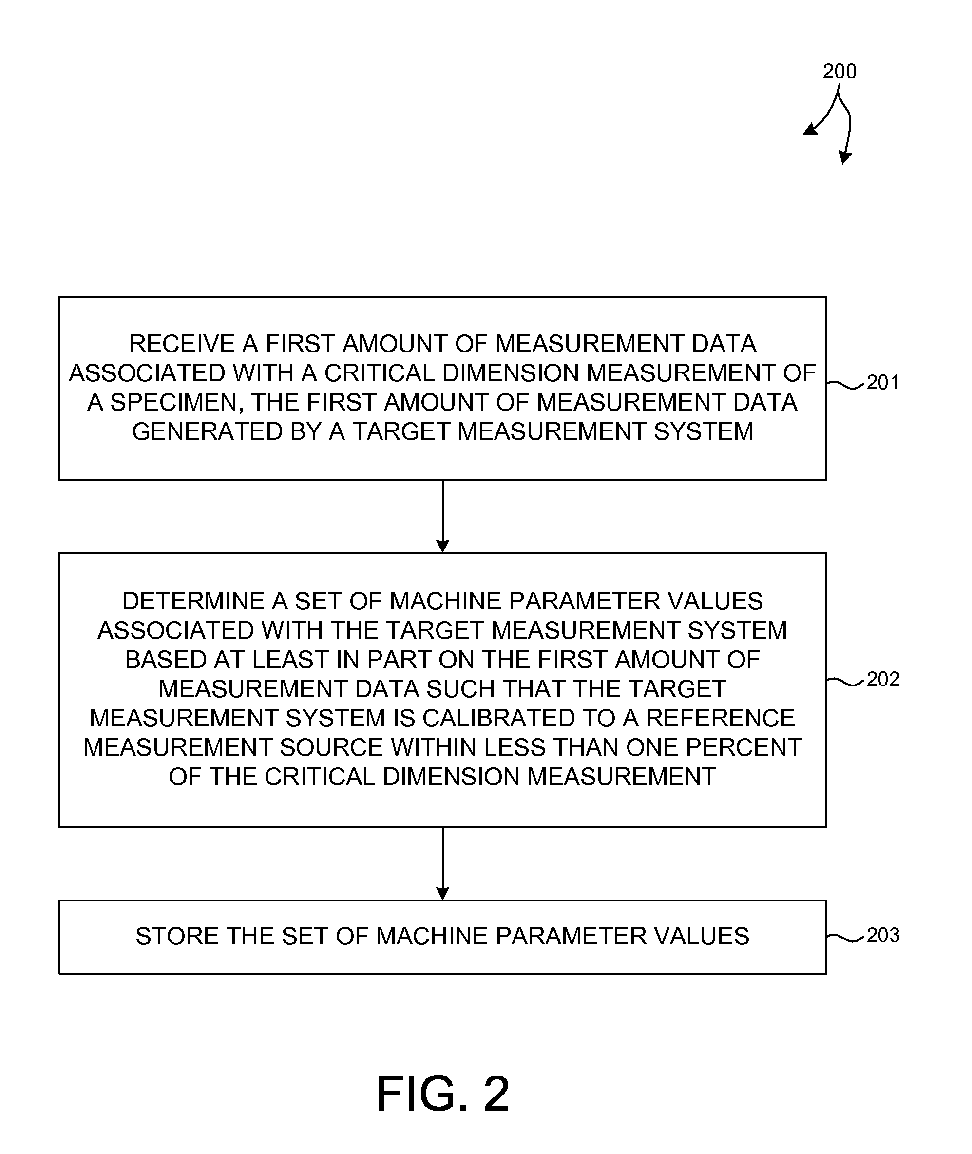
[0017]Methods and systems for matching critical dimension measurement applications across one or more optical metrology systems are presented. Such systems are employed to measure structural and material characteristics (e.g., material composition, dimensional characteristics of structures and films, etc.) associated with different semiconductor fabrication processes.

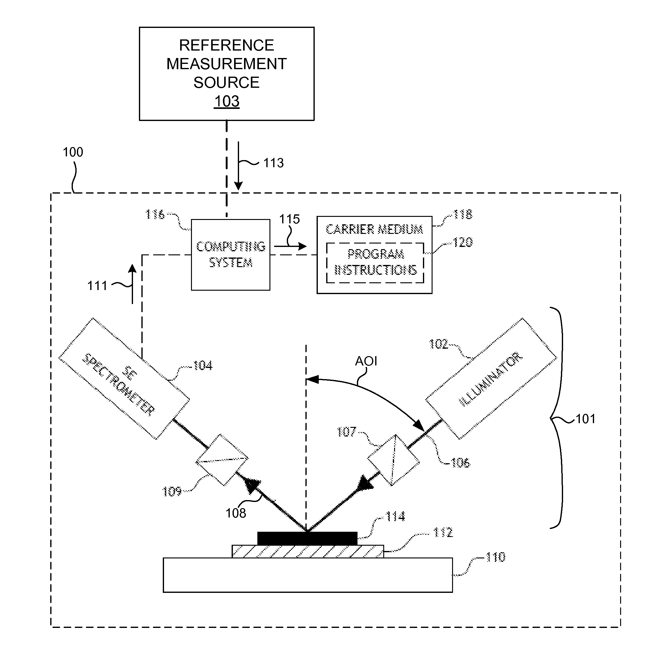
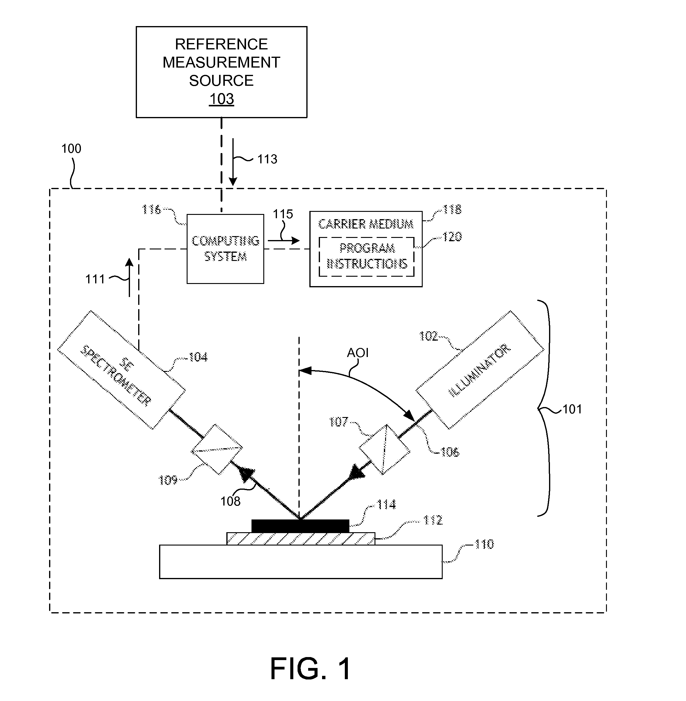
[0018]FIG. 1 illustrates a system 100 for measuring characteristics of a semiconductor wafer in accordance with the exemplary methods presented herein. As shown in FIG. 1, the system 100 may be used to perform spectroscopic ellipsometry measurements of one or more structures 114 of a semiconductor wafer 112 disposed on a wafer positioning system 110. In this aspect, the system 100 may include a spectroscopic ellipsometer equipped with an illuminator 102 a...


PUM


Abstract

Methods and systems for matching critical dimension measurement applications at high precision across multiple optical metrology systems are presented. In one aspect, machine parameter values of a metrology system are calibrated based on critical dimension measurement data. In one further aspect, calibration of the machine parameter values is based on critical dimension measurement data collected by a target measurement system from a specimen with assigned critical dimension parameter values obtained from a reference measurement source. In another further aspect, the calibration of the machine parameter values of a target measurement system is based on measurement data without knowledge of critical dimension parameter values. In some examples, the measurement data includes critical dimension measurement data and thin film measurement data. Calibration of machine parameter values based on critical dimension data enhances application and tool-to-tool matching among systems for measurement of critical dimensions, film thickness, film composition, and overlay.

Description

CROSS REFERENCE TO RELATED APPLICATION[0001]The present application for patent claims priority under 35 U.S.C. §119 from U.S. provisional patent application Ser. No. 61 / 610,626, entitled “Calibration Of An Optical Metrology System For CD / Application Matching,” filed Mar. 14, 2012, the subject matter of which is incorporated herein by reference in its entirety.TECHNICAL FIELD[0002]The described embodiments relate to optical metrology systems and methods, and more particularly to methods and systems for improved consistency across critical dimension measurement applications.BACKGROUND INFORMATION[0003]Semiconductor devices such as logic and memory devices are typically fabricated by a sequence of processing steps applied to a specimen. The various features and multiple structural levels of the semiconductor devices are formed by these processing steps. For example, lithography among others is one semiconductor fabrication process that involves generating a pattern on a semiconductor w...

Claims


Application Information

Patent Timeline
IPC IPC(8): G05B23/00
CPCG05B23/00G03F7/70625G03F7/70608G03F7/706845G03F7/706839
Inventor FLOCK, KLAUSROTTER, LAWRENCEARAIN, MUZAMMIL
Owner KLA TENCOR TECH CORP
Why Eureka
Try Eureka