

Method of fabricating nonpolar gallium nitride-based semiconductor layer, nonpolar semiconductor device, and method of fabricating the same
- Summary
- Abstract
- Description
- Claims
- Application Information
AI Technical Summary
Benefits of technology
Problems solved by technology
Method used
Image

Examples
experimental example 1
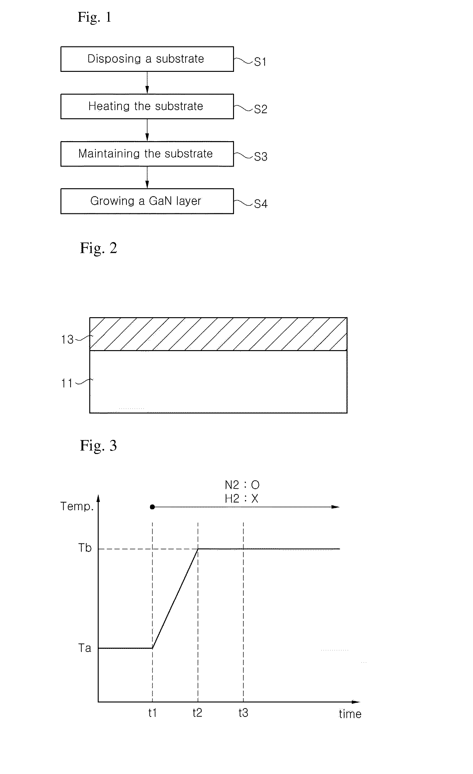
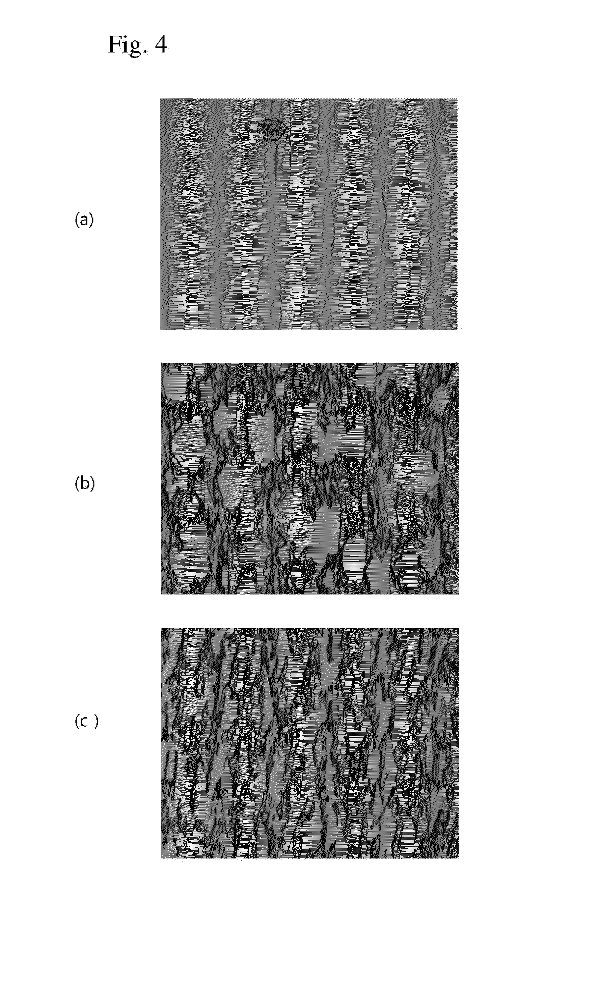
[0053]FIGS. 4A to 4C are optical photographs showing surface morphologies of the nonpolar gallium nitride layer 13 according to kinds of ambient gas. Specifically, FIG. 4A shows the case where N2 is supplied as the ambient gas, FIG. 4B shows the case where H2 is supplied as the ambient gas, and FIG. 4C shows the case where N2 and H2 are supplied together as the ambient gas. In all the cases, the gallium nitride layer was grown on the m-plane gallium nitride substrate 11 at the same growth temperature, and flow rates of source gases were adjusted appropriately to each ambient gas.
[0054]As shown in FIG. 4A, in a case where H2 was not supplied and N2 was supplied as the ambient gas, the gallium nitride layer 13 with relatively excellent surface morphology was grown. On the other hand, as shown in FIGS. 4B and 4C, in a case where H2 was contained in the ambient gas, the surface of the gallium nitride layer was very rough. In addition, in a case where only H2 was supplied, the surface of...
experimental example
[0093]FIGS. 13A to 13C are optical photographs showing surface morphologies of the epitaxial layer according to the use of the intermediate-temperature buffer layer 113. FIG. 13A is a photograph showing the surface of the n-type GaN layer grown on the gallium nitride substrate 111, without the intermediate-temperature buffer layer 113. FIG. 13B is a photograph showing the surface of the n-type GaN layer immediately grown when the intermediate-temperature buffer layer 113 was formed on the gallium nitride substrate 111, the substrate temperature was raised to the growth temperature of the n-type GaN layer and then reached the growth temperature of the n-type GaN layer. FIG. 13C is a photograph showing the surface of the n-type GaN layer grown when the intermediate-temperature buffer layer 113 was formed on the gallium nitride substrate 111, the substrate temperature was raised to the growth temperature of the n-type GaN layer and then the intermediate-temperature buffer layer was mai...
PUM
 Abstract
Description
Claims
Application Information