
Metrology Method and Apparatus, Lithographic System and Device Manufacturing Method

Active Publication Date: 2013-10-03
ASML NETHERLANDS BV
View PDF2 Cites 437 Cited by
  • Summary
  • Abstract
  • Description
  • Claims
  • Application Information

AI Technical Summary

Benefits of technology

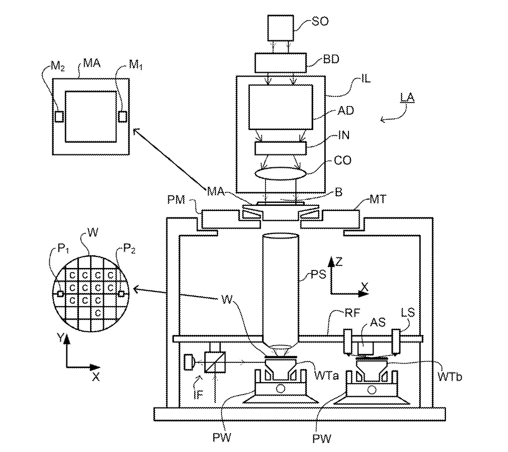
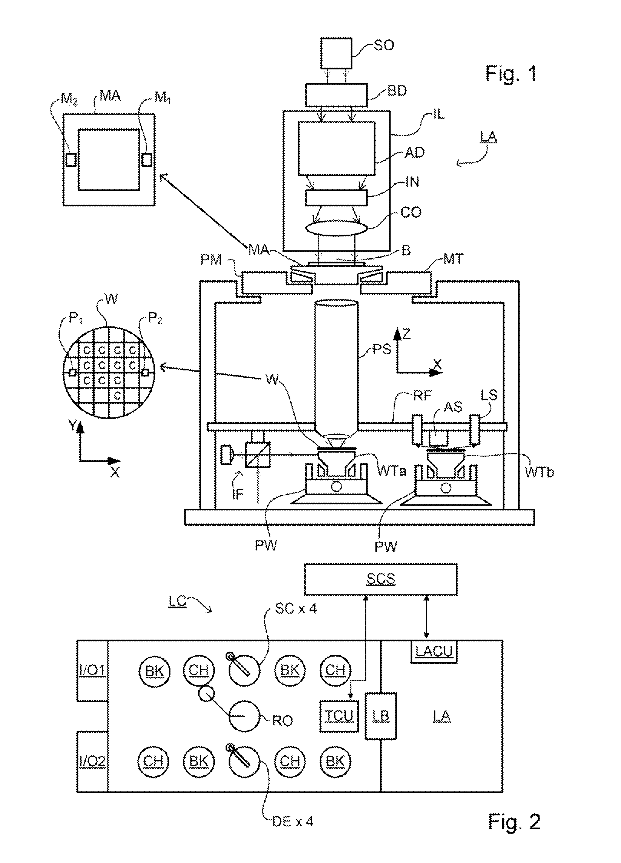
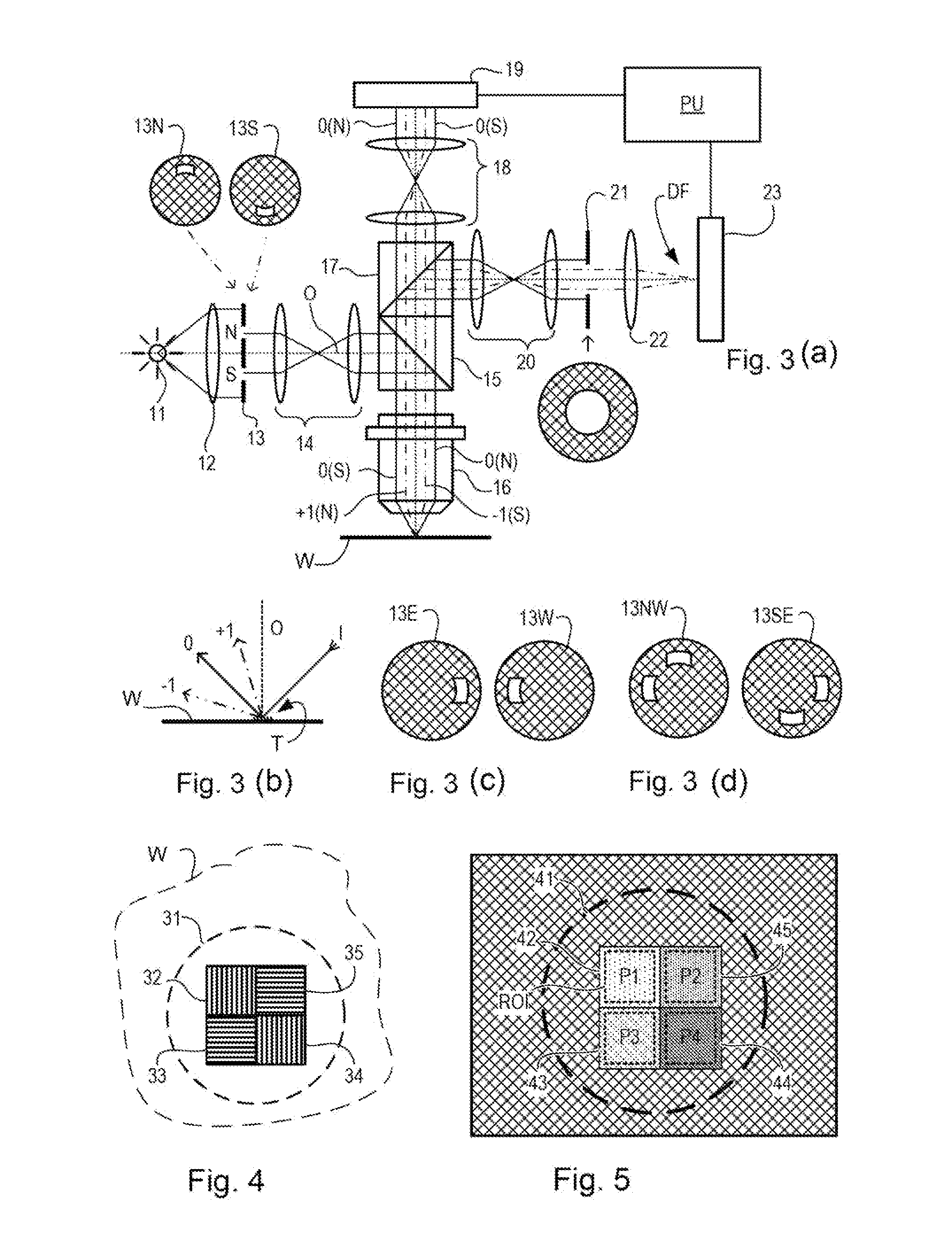
The patent text describes a method and apparatus for measuring the asymmetry of a target structure caused by overlay and other effects. The goal is to improve accuracy and throughput compared to previous methods. The invention may also be used for small target structures that can be read out using the dark-field image-based technique.

Problems solved by technology

Although the known dark-field image-based overlay measurements are fast and computationally very simple (once calibrated), they rely on an assumption that overlay is the only cause of asymmetry in the target structure.
This asymmetry which is not related to the overlay clearly perturbs the overlay measurement, giving an inaccurate overlay result.
Accordingly at this time the skilled person has to choose between, on the one hand, a simple and fast measurement process that gives overlay measurements but is subject to inaccuracies when other causes of asymmetry are present, and on the other hand more traditional techniques that are computationally intensive and typically require several measurements of large, underfilled gratings to avoid the pupil image is polluted with signal from the environment of the overlay grating, which hampers the reconstruction on this.

Method used


Image

  • Metrology Method and Apparatus, Lithographic System and Device Manufacturing Method
  • Metrology Method and Apparatus, Lithographic System and Device Manufacturing Method
  • Metrology Method and Apparatus, Lithographic System and Device Manufacturing Method

Examples


example 1

Solving for K0, K1, and ov with 3 gratings

[0092]Target (a) in FIG. 9 includes three component gratings with a symmetric bias scheme (−d, 0, and +d). To solve for the first harmonic and for a constant asymmetry signal coming from the bottom-grating asymmetry (BGA) we can write:

ΔI+=K0+K1·sin(ov+d)

ΔI0=K0+K1·sin(ov)

ΔI−=K0+K1·sin(ov−d)

where ΔI is the intensity difference representing the measured asymmetry and the suffix ‘+’, ‘0’ or ‘−’ indicates the bias.

[0093]The solution of this set of equations can be written as:

ov=atan{[ΔI++ΔI--2ΔI0]·sin(d)[ΔI+-ΔI-]·(cos(d)-1)}K0=ΔI++ΔI--2ΔI0·cos(d)2·(1-cos(d))K1=[ΔI+-ΔI-]2·sin(d)·1+([ΔI++ΔI--2ΔI0]·sin(d)[ΔI+-ΔI-]·(cos(d)-1))2

[0094]This gives a direct calculation of the overlay, taking a constant asymmetry offset into account for the BGA or other feature asymmetry. We suggest to use a range of bias that is a significant proportion of the grating pitch P, to ensure that the curvature of the sine function is captured by the three sample points, and is...

example 2

Solving for K0, K1, and ov with 4 gratings

[0095]For the targets with four biased gratings, shown in FIGS. 9 (b), (c) and (d), the following equations can be written:

ΔI−d−Δd=K0+K1·sin(ov−d−Δd)

ΔI−d+Δd=K0+K1·sin(ov−d+Δd)

ΔI+d−Δd=K0+K1·sin(ov+d−Δd)

ΔI+d+Δd=K0+K1·sin(ov+d+Δd)

[0096]Solving for the unknown parameters yields:

ov=atan{((ΔI-d+Δd-ΔI-d-Δd)-(ΔI+d+Δd-ΔI+d-Δd))·sin(d-Δd)2·(ΔI+d-Δd-ΔI-d+Δd)·sin(d)·sin(Δd)}K0=(ΔI+d+Δd+ΔI-d-Δd)·cos(d-Δd)-(ΔI+d-Δd+ΔI-d+Δd)·cos(d+Δd)2·(cos(d+Δd)-cos(d-Δd))K1=(ΔI+d-Δd-ΔI-d+Δd)2·sin(d-Δd)×1+(((ΔI-d+Δd-ΔI-d-Δd)-(ΔI+d+Δd-ΔI+d-Δd))·sin(d-Δd)2·(ΔI+d-Δd-ΔI-d+Δd)·sin(d)·sin(Δd))2

[0097]Again, the range of biases should be significant as a proportion of the grating pitch P. For example it is suggested to use in this case a bias d=40 nm and a sub-bias Δd=20 nm, where the pitch P=500 nm. The biases thus range from +60 nm to −60 nm, that is a range of 120 nm overall. Here also, this is relatively large, representing more than 20% but less than 9% of the pitch, and wil...

example 3

Solving for K0, K1, K2, and ov with 4 gratings and 2nd harmonic

[0098]For the 4-gratings per target case above, also the second harmonic can be included if the design of the gratings and the optical system requires it. We can write:

ΔI−d−Δd=K0+K1·sin(ov−d−Δd)+K2·sin(2·(ov−d−Δd))

ΔI−d+Δd=K0+K1·sin(ov−d+Δd)+K2·sin(2·(ov−d+Δd))

ΔI+d−Δd=K0+K1·sin(ov+d−Δd)+K2·sin(2·(ov+d−Δd))

ΔI+d+Δd=K0+K1·sin(ov+d+Δd)+K2·sin(2·(ov+d+Δd))

[0099]To solve this set of equations we defining some new parameters as:

ΔIa=ΔI+d+Δd-ΔI-d-ΔdΔIb=ΔI+d-Δd-ΔI+d-ΔdΔIc=(ΔI+d+Δd-ΔI+d-Δd)-(ΔI-d+Δd-ΔI-d-Δd)wherea1=2·sin(d+Δd)a2=2·sin(2·(d+Δd))b1=2·sin(d-Δd)b2=2·sin(2·(d-Δd))c1=-4·sin(d)·sin(Δd)c2=-4·sin(2d)·sin(2Δd)andz0=(a1b2-a2b1)·ΔIcc1·(b2ΔIa-a2ΔIb)z1=(2·b1c2-b2c1)·ΔIa+(a2c1-2·a1c2)·ΔIbc1·(b2ΔIa-a2ΔIb)Q=3·z1-z029R=2·z02-9·z0·(z1+3)54D=Q3+R2S=R+Q3T=R-Q3

[0100]The equations can then be solved, yielding three possible solutions:

ov1=atan{z03+(S+T)}ov2=atan{z03-12(S+T)+12·i·3(S-T)}ov3=atan{z03-12(S+T)-12·i·3(S-T)}

[0101]Of these result...


PUM

PropertyMeasurementUnit
Fractionaaaaaaaaaa
Fractionaaaaaaaaaa
Fractionaaaaaaaaaa

Abstract

A lithographic process is used to form a plurality of target structures (T) on a substrate (W). Each target structure comprises overlaid gratings each having a specific overlay bias. Asymmetry (A) of each grating, measured by scatterometry, includes contributions due to (i) the overlay bias, (ii) an overlay error (OV) in the lithographic process and (iii) bottom grating asymmetry within the overlaid gratings. Asymmetry measurements are obtained for three or more target structures having three or more different values of overlay bias (e.g., −d, 0, +d). Knowing the three different overlay bias values and a theoretical curve relationship between overlay error and asymmetry, overlay error (OV) can be calculated while correcting the effect of bottom grating asymmetry. Bias schemes with three and four different biases are disclosed as examples. Gratings with different directions and biases can be interleaved in a composite target structure.

Description

BACKGROUND[0001]1. Field of the Invention[0002]The present invention relates to methods and apparatus for metrology usable, for example, in the manufacture of devices by lithographic techniques and to methods of manufacturing devices using lithographic techniques.[0003]2. Background Art[0004]A lithographic apparatus is a machine that applies a desired pattern onto a substrate, usually onto a target portion of the substrate. A lithographic apparatus can be used, for example, in the manufacture of integrated circuits (ICs). In that instance, a patterning device, which is alternatively referred to as a mask or a reticle, may be used to generate a circuit pattern to be formed on an individual layer of the IC. This pattern can be transferred onto a target portion (e.g., including part of, one, or several dies) on a substrate (e.g., a silicon wafer). Transfer of the pattern is typically via imaging onto a layer of radiation-sensitive material (resist) provided on the substrate. In general...

Claims


Application Information

Patent Timeline
IPC IPC(8): G01N21/956G03F9/00
CPCG03F7/70633G03F7/70683Y10T428/24802G03F9/7019G01N21/956H01L22/12
Inventor SMILDE, HENDRIK JAN HIDDEADAM, OMER ABUBAKER OMER
Owner ASML NETHERLANDS BV
Learn More