Eddy current sensor and polishing method

a technology of eddy current sensor and polishing method, which is applied in the direction of semiconductor/solid-state device testing/measurement, lapping machines, instruments, etc., can solve the problems of stability of characteristics, influence of circuit noise becomes greater, and the capacitor component between lines can be small, improve the sensitivity of the sensor, and shorten the processing time

Active Publication Date: 2013-10-03
EBARA CORP
View PDF4 Cites 12 Cited by
  • Summary
  • Abstract
  • Description
  • Claims
  • Application Information

AI Technical Summary

Benefits of technology

[0056]4) Since the detection coil of the eddy current sensor comprises a coil formed by winding a wire or a conductive material in a single row and plural layers, the detection coil can be brought close to the substrate, and capacitance component between lines can be small, thus improving sensor sensitivity. Therefore, the thin metal film (or thin conductive film) on the substrate such as a semiconductor wafer can be detected without increasing oscillation frequency, amplification degree of an internal circuit and exciting voltage of the eddy current sensor.
[0057]5) In the case where the remaining film is detected by performing an inspection on whether or not there is a remaining film such as a metal film (or conductive film) on a substrate during polishing, additional polishing is performed as it is, and thus processing time can be shortened. Further, in the case where the remaining film is detected, because the controller for controlling the entire CMP process controls additional polishing time or the remaining film condition, it is possible to change the polishing condition of the subsequent object to be polished to the optimum condition.

Problems solved by technology

In the case where the oscillation frequency is set around the coil resonance frequency, there is a problem of stability of characteristics.
Further, in the case where the amplification degree of the internal circuit of the eddy current sensor is increased, influence of a circuit noise becomes greater.
Further, in the case where the exciting voltage of the eddy current sensor is increased, there is a problem of stability of characteristics.

Method used


Image

  • Eddy current sensor and polishing method
  • Eddy current sensor and polishing method
  • Eddy current sensor and polishing method

Examples


Embodiment Construction

[0101]A polishing apparatus according to embodiments of the present invention will be described below with reference to FIGS. 1 through 31. Like or corresponding structural elements are denoted by like or corresponding reference numerals in FIGS. 1 through 31 and will not be described below repetitively.

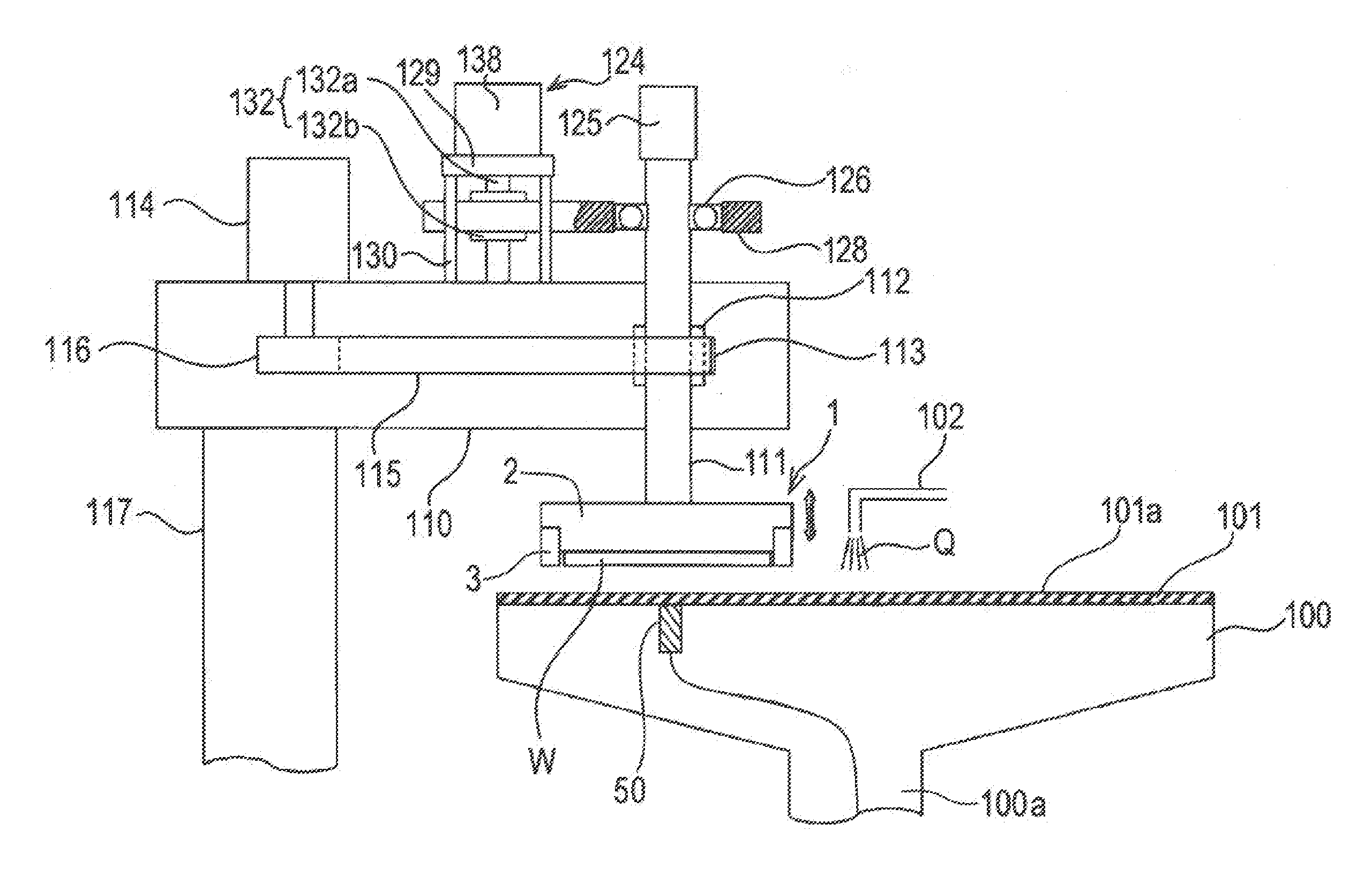
[0102]FIG. 1 is a schematic view showing an entire structure of a polishing apparatus according to the present invention. As shown in FIG. 1, the polishing apparatus comprises a polishing table 100, and a top ring 1 for holding a substrate such as a semiconductor wafer as an object to be polished and pressing the substrate against a polishing surface on the polishing table.

[0103]The polishing table 100 is coupled via a table shaft 100a to a motor (not shown) disposed below the polishing table 100. Thus, the polishing table 100 is rotatable about the table shaft 100a. A polishing pad 101 is attached to an upper surface of the polishing table 100. An upper surface 101a of the polishing...


PUM

PropertyMeasurementUnit
distanceaaaaaaaaaa
conductiveaaaaaaaaaa
sizesaaaaaaaaaa

Abstract

An eddy current sensor is used for detecting a metal film (or conductive film) formed on a surface of a substrate such as a semiconductor wafer. The eddy current sensor is disposed near the metal film or the conductive film formed on the substrate to detect an eddy current generated in the metal film or the conductive film. The eddy current sensor includes a plurality of coils having different sizes formed by winding a wire or a conductive material. The plurality of coils includes an inner coil and an outer coil spaced from each other, and the outer coil is configured to surround the inner coil. The plurality of coils are configured to detect respective eddy currents generated in the metal film or the conductive film.

Description

CROSS REFERENCE TO RELATED APPLICATIONS[0001]This document claims priority to Japanese Application Number 2012-079555, filed Mar. 30, 2012, the entire contents of which are hereby incorporated by reference.BACKGROUND OF THE INVENTION[0002]1. Field of the Invention[0003]The present invention relates to an eddy current sensor suitable for detecting a metal film (or conductive film) formed on a surface of a substrate such as a semiconductor wafer. Further, the present invention relates to a polishing method and apparatus for polishing the substrate while monitoring the metal film (or conductive film) formed on the substrate by the eddy current sensor to remove the metal film (or conductive film).[0004]2. Description of the Related Art[0005]In recent years, high integration and high density in semiconductor device demands smaller and smaller wiring patterns or interconnections and also more and more interconnection layers. Multilayer interconnections in smaller circuits result in greate...

Claims


Application Information

Patent Timeline
Patent Type & Authority Applications(United States)
IPC IPC(8): G01N27/90B24B49/10
CPCG01N27/90B24B49/105H01L22/14B24B37/013H01L2924/0002H01L22/26H01L2924/00B24B37/04G01N27/72G01N27/82
Inventor TAKAHASHI, TAROTADA, MITSUO
Owner EBARA CORP
Why Eureka
Try Eureka