Insulating film, method for manufacturing semiconductor device, and semiconductor device

Active Publication Date: 2013-10-10
SEMICON ENERGY LAB CO LTD
View PDF3 Cites 69 Cited by
  • Summary
  • Abstract
  • Description
  • Claims
  • Application Information

AI Technical Summary

Benefits of technology

[0017]In a transistor including an oxide semiconductor, an oxide insulating film containing oxygen in excess of the stoichiometric composition is formed as a protective film formed over the transistor, and the oxygen in the protective film is diffused to the oxide

Problems solved by technology

In a transistor using an oxide semiconductor, oxygen vacancies (oxygen defects) in an oxide semiconductor film cause defects of electric characteristics of the transistor.
In addition, a transistor using an oxide sem

Method used


Image

  • Insulating film, method for manufacturing semiconductor device, and semiconductor device
  • Insulating film, method for manufacturing semiconductor device, and semiconductor device
  • Insulating film, method for manufacturing semiconductor device, and semiconductor device

Examples


embodiment 1

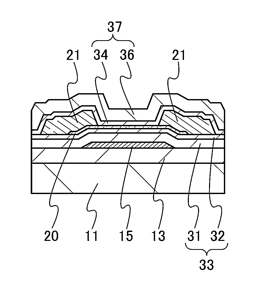
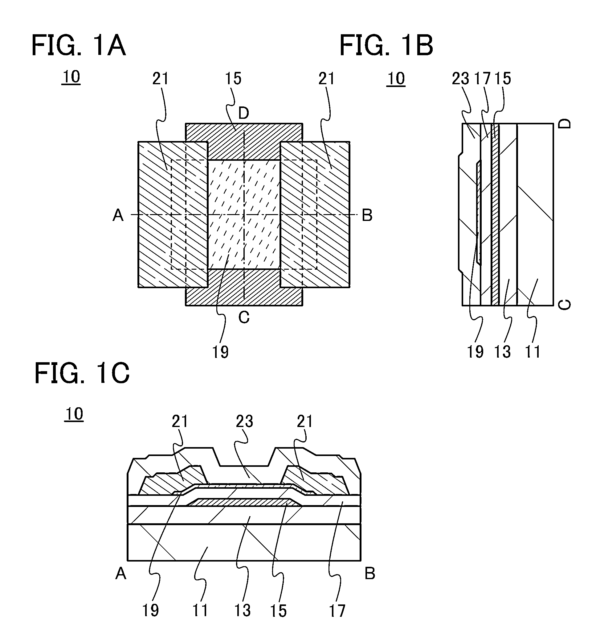
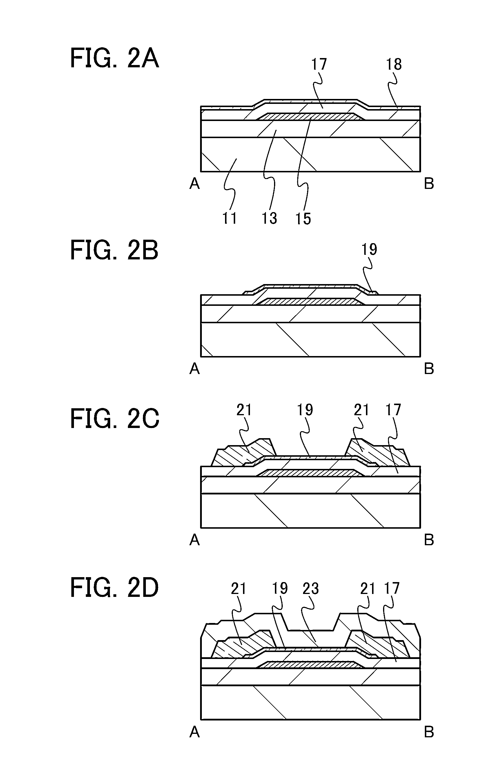
[0052]In this embodiment, a semiconductor device which is one embodiment of the present invention, and a method for manufacturing the semiconductor device will be described with reference to drawings.

[0053]FIGS. 1A to 1C are a top view and cross-sectional views of a transistor 10 included in a semiconductor device. FIG. 1A is a top view of the transistor 10, FIG. 1B is a cross-sectional view taken along dashed-dotted line A-B in FIG. 1A, and FIG. 1C is a cross-sectional view taken along dashed-dotted line C-D in FIG. 1A. Note that in FIG. 1A, some components of the transistor 10 (e.g., a substrate 11, a base insulating film 13, and a gate insulating film 17), a protective film 23, and the like are not illustrated for simplicity.

[0054]The transistor 10 illustrated in FIGS. 1B and 1C includes a gate electrode 15 over the base insulating film 13, the gate insulating film 17 over the base insulating film 13 and the gate electrode 15, an oxide semiconductor film 19 overlapping with the g...

embodiment 2

[0161]In this embodiment, a transistor having a different structure from the transistor in Embodiment 1 will be described with reference to FIGS. 5A to 5C. A transistor 100 shown in this embodiment is a top-gate transistor, which is different from the transistor shown in Embodiment 1.

[0162]FIG. 5A to 5C are a top view and cross-sectional views of the transistor 100.

[0163]FIG. 5A is a top view of the transistor 100, FIG. 5B is a cross-sectional view taken along dashed-dotted line A-B in FIG. 5A, and FIG. 5C is a cross-sectional view taken along dashed-dotted line C-D in FIG. 5A. Note that in FIG. 5A, some components of the transistor 100 (e.g., a substrate 101, a base insulating film 103, and a gate insulating film 109), a protective film 113, and the like are not illustrated for simplicity.

[0164]The transistor 100 illustrated in FIGS. 5B and 5C includes an oxide semiconductor film 105 over the base insulating film 103, a pair of electrodes 107 in contact with the oxide semiconductor...

embodiment 3

[0214]In this embodiment, a transistor having a structure different from those of Embodiment 1 and Embodiment 2 will be described with reference to FIGS. 7A and 7B. A transistor 120 shown in this embodiment is different from the transistor 100 shown in Embodiment 2 in that dopant is added to an oxide semiconductor film.

[0215]FIGS. 7A and 7B are a top view and a cross-sectional view of the transistor 120. FIG. 7A is a top view of the transistor 120, and FIG. 7B corresponds to a cross-sectional view taken along dashed line A-B in FIG. 7A. Note that in FIG. 7A, some components of the transistor 120 (e.g., a substrate 101, a base insulating film 103, and a gate insulating film 109), a protective film 113, and the like are not illustrated for simplicity.

[0216]The transistor 120 illustrated in FIG. 7B includes an oxide semiconductor film 121 over the base insulating film 103, a pair of electrodes 107 in contact with the oxide semiconductor film 121, the gate insulating film 109 in contact...


PUM


Abstract

In a semiconductor device including a transistor including an oxide semiconductor film and a protective film over the transistor, an oxide insulating film containing oxygen in excess of the stoichiometric composition is formed as the protective film under the following conditions: a substrate placed in a treatment chamber evacuated to a vacuum level is held at a temperature higher than or equal to 180° C. and lower than or equal to 260° C.; a source gas is introduced into the treatment chamber so that the pressure in the treatment chamber is set to be higher than or equal to 100 Pa and lower than or equal to 250 Pa; and a high-frequency power higher than or equal to 0.17 W/cm2 and lower than or equal to 0.5 W/cm2 is supplied to an electrode provided in the treatment chamber.

Description

TECHNICAL FIELD[0001]The present invention relates to a method for forming an insulating film and a method for manufacturing a semiconductor device including a field-effect transistor.BACKGROUND ART[0002]Transistors used for most flat panel displays typified by a liquid crystal display device and a light-emitting display device are formed using silicon semiconductors such as amorphous silicon, single crystal silicon, and polycrystalline silicon provided over glass substrates. Further, transistors formed using such silicon semiconductors are used in integrated circuits (ICs) and the like.[0003]In recent years, attention has been drawn to a technique in which, instead of a silicon semiconductor, a metal oxide exhibiting semiconductor characteristics is used for transistors. Note that in this specification, a metal oxide exhibiting semiconductor characteristics is referred to as an oxide semiconductor.[0004]For example, a technique is disclosed, in which a transistor is manufactured us...

Claims


Application Information

Patent Timeline
IPC IPC(8): H01L29/66H01L29/786
CPCH01L29/66742H01L29/7869H01L29/66969H01L21/02274H01L21/02112H01L29/0684H01L29/66477H01L29/78H01L29/78696H01L29/78606H01L29/24H01L29/4908H01L29/4966H01L29/78648H01L21/385H01L23/3171H01L29/045H01L29/45
Inventor OKAZAKI, KENICHISASAKI, TOSHINARIYOKOYAMA, SHUHEIHAMOCHI, TAKASHI
Owner SEMICON ENERGY LAB CO LTD
Why Eureka
Try Eureka