Supercharge Your Innovation With Domain-Expert AI Agents!

Semiconductor device having plural data input/output terminals

a technology of data input/output terminals and semiconductors, applied in the field of semiconductor devices, can solve the problem that arbitrary test data cannot be written to each of the data input/output terminals

Active Publication Date: 2013-10-10
NVIDIA CORP
View PDF8 Cites 7 Cited by
  • Summary
  • Abstract
  • Description
  • Claims
  • Application Information

AI Technical Summary

Benefits of technology

The patent text describes various embodiments of semiconductor devices and memory cell arrays with improved test circuit units and a buffer circuit for efficient data input / output. The technical effects of these embodiments include improved data processing speed, reduced latency, and improved reliability of data transfer. Additionally, the patent describes an auxiliary circuit that can further enhance the efficiency of data transfer and processing. Overall, the patent aims to provide improved performance and reliability for semiconductor devices and memory cell arrays.

Problems solved by technology

When the screening test described in Japanese Patent Application Laid-open No. 2001-57100 is adapted to the final test in a wafer state, the tester can receive read data not being compressed; however, arbitrary test data cannot be written to each of the data input / output terminals.

Method used


Image

  • Semiconductor device having plural data input/output terminals
  • Semiconductor device having plural data input/output terminals
  • Semiconductor device having plural data input/output terminals

Examples


Embodiment Construction

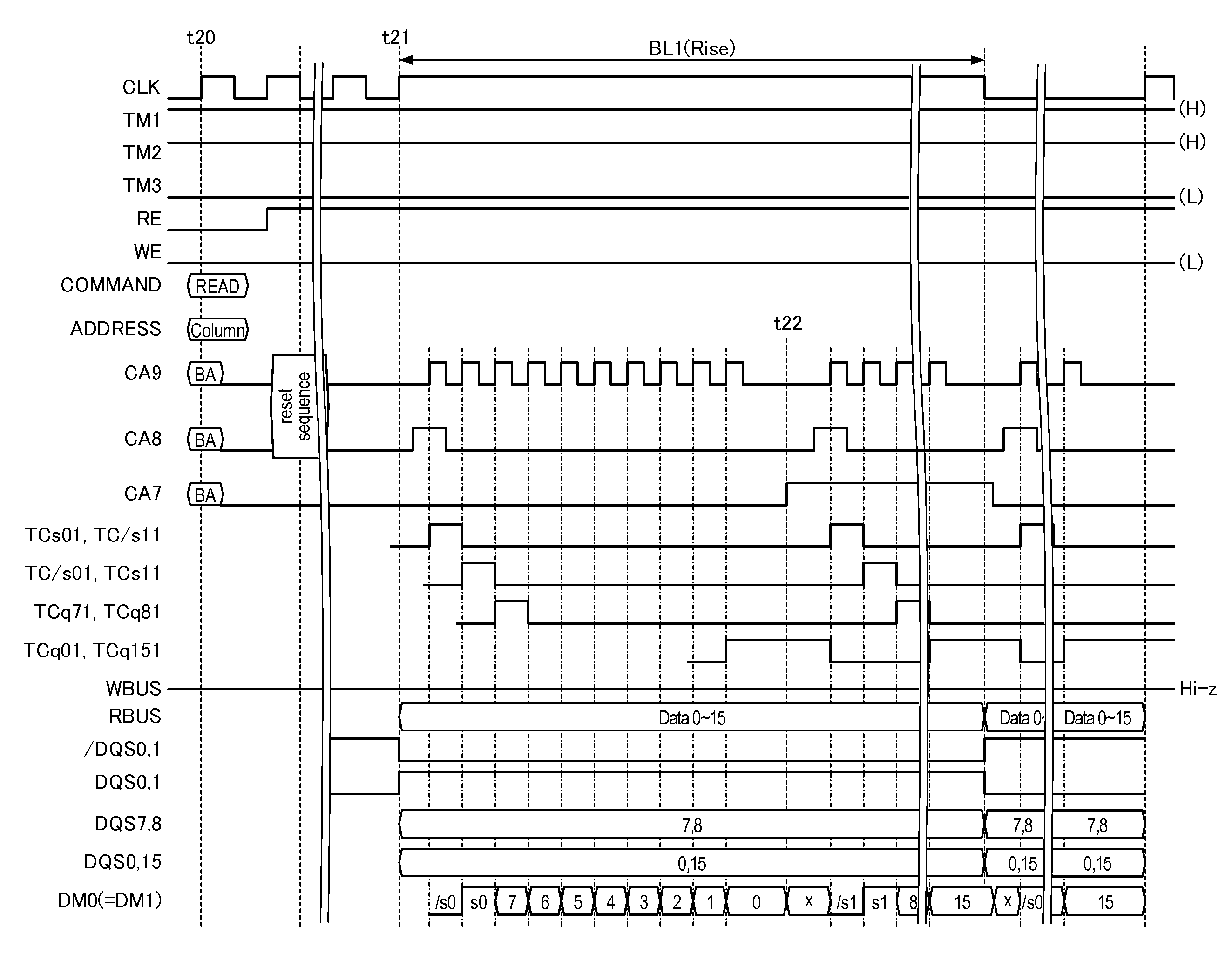
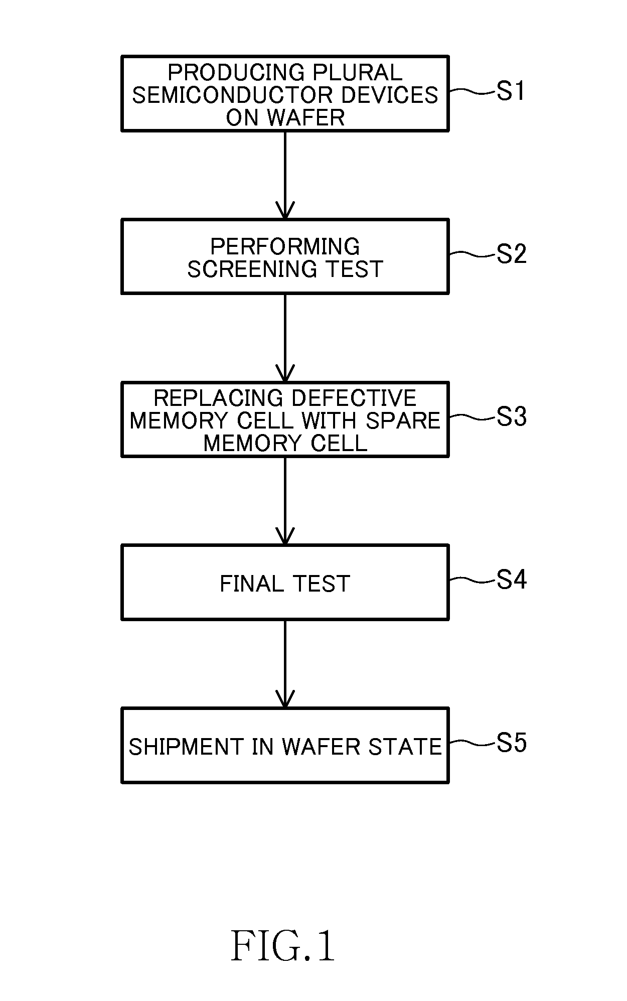
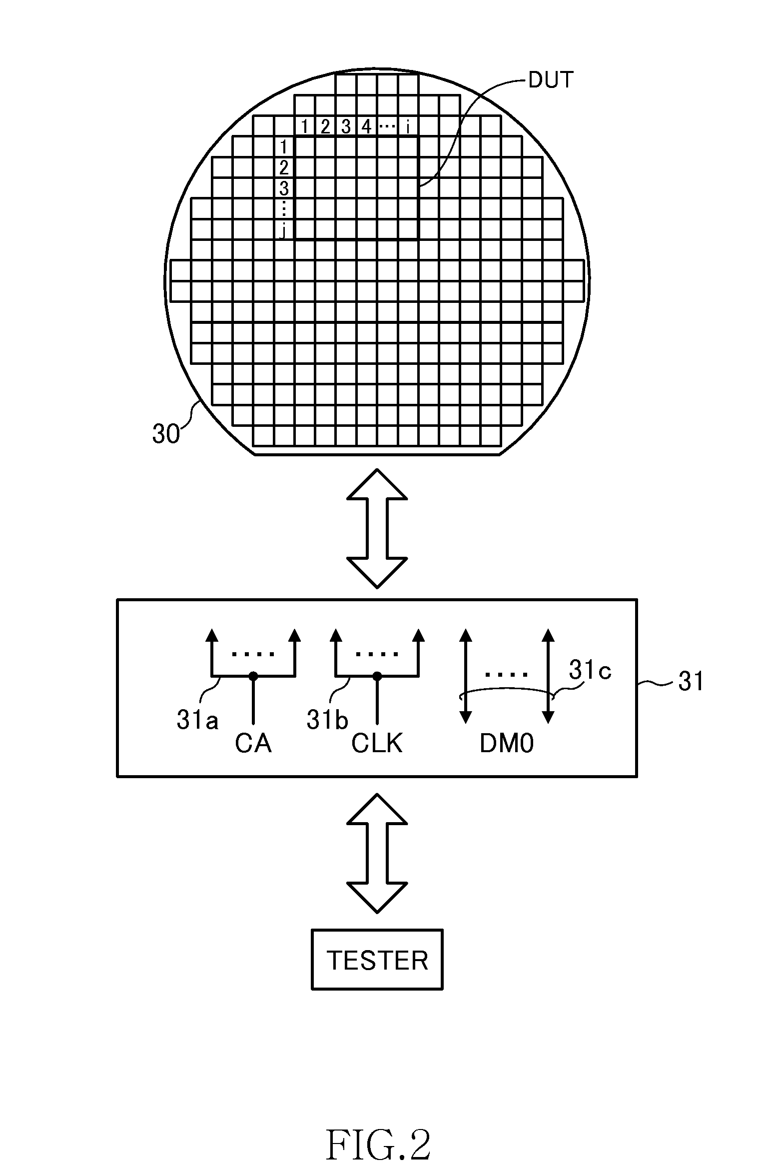
[0027]Referring now to FIG. 1, in a manufacturing process of a semiconductor device, a large number of semiconductor devices are produced on a wafer (Step S1) and then a screening test is performed in a wafer state (Step S2), Semiconductor devices are produced in a process of forming devices by performing ion implantation to a wafer made of silicon, formation of a conductive film and an insulating film on the wafer, patterning of these films, and the like. Although not particularly limited thereto, the semiconductor devices produced in the present embodiment are DRAMs and therefore many memory cells are formed in each of the semiconductor devices on the wafer. The screening test is a process of determining whether a read operation and a write operation can be correctly performed to these memory cells. A defective memory cell found in the screening test is replaced by a spare memory cell. In this way, an address corresponding to the defective memory cell is relieved (Step S3).

[0028]A...


PUM


Abstract

Disclosed herein is a device that includes a plurality of first terminals; a first circuit including a plurality of first nodes; a buffer circuit including a plurality of second nodes connected to the first terminals through a plurality of first interconnection lines, respectively, and a plurality of third nodes connected to the first nodes of the first circuit through a plurality of second interconnection lines, respectively; and a second circuit configured to perform at least one of first and second operations. The first operation is such that a plurality of first signals, that appear respectively on the first interconnection lines, are outputted in series, and the second operation is such that a plurality of second signals, that are supplied in series, are transferred respectively to the first interconnection lines.

Description

BACKGROUND OF THE INVENTION[0001]1. Field of the Invention[0002]The present invention relates to a semiconductor device and a test method therefor, and more particularly relates to a semiconductor device including a plurality of data input / output terminals and a test method therefor.[0003]2. Description of Related Art[0004]Various operation tests are performed at each step in a process of manufacturing a semiconductor device. For example, Japanese Patent Application Laid-open No. H5-74898 discloses that a screening test of a semiconductor memory device such as a DRAM (Dynamic Random Access Memory) is performed in a wafer state and then a final test is performed for a packaged semiconductor memory device. It is desirable that the screening test in a wafer state be executed for many semiconductor memory devices in parallel. However, if all data input / output terminals thereof are connected to a probe card, fewer semiconductor memory devices can be tested in parallel and accordingly a m...

Claims


Application Information

Patent Timeline
Patent Type & Authority Applications(United States)
IPC IPC(8): G01R31/28G11C7/10
CPCG01R31/2894G11C7/10G11C29/006G11C11/401G11C29/32G11C2029/5602G11C29/1201
Inventor MIYAJI, TEPPEIMATSUI, YOSHINORI
Owner NVIDIA CORP
Features
  • R&D
  • Intellectual Property
  • Life Sciences
  • Materials
  • Tech Scout
  • Unparalleled Data Quality
  • Higher Quality Content
  • 60% Fewer Hallucinations
Learn More