Check patentability & draft patents in minutes with Patsnap Eureka AI!

Method of Fabricating An Electromechanical Structure Including at Least One Mechanical Reinforcing Pillar

a technology of mechanical reinforcement and electromechanical structure, which is applied in the direction of microelectromechanical systems, microstructural technology, electric devices, etc., can solve the problems of poor mechanical integrity, poor control of shape, and risk of revealing the bonding interface, so as to avoid the drawback of any revealing risk and limit the topology

Active Publication Date: 2013-10-17
COMMISSARIAT A LENERGIE ATOMIQUE ET AUX ENERGIES ALTERNATIVES
View PDF4 Cites 0 Cited by
  • Summary
  • Abstract
  • Description
  • Claims
  • Application Information

AI Technical Summary

Benefits of technology

Enables the fabrication of pillars with widths up to several tens of micrometers, providing enhanced mechanical integrity and versatility in electromechanical structures without the limitations of traditional methods, while maintaining control over the bonding interface.

Problems solved by technology

During that operation, the interface zone between the added substrate and the remainder of the structure is subjected to chemical etching (in general with HF acid), thereby leading to shapes that are poorly controlled if the interface is not perfect, since the speed of etching is variable, and there is a risk of revealing the bonding interface.
After the sacrificial layer has been removed, and the MEMS structure has been released, mechanical integrity is not good.
Nevertheless, the pillars are made of thick poly-Si and their lateral size is limited by the technology.
Known methods are therefore limited to pillars of width that is limited to the thickness of the poly-Si layer used for filling them.
Since the stress state of polycrystalline Si (at the time of deposition or during heating) is different from that of SiO2, limiting the lateral dimensions of the pillars serves to limit non-uniformities in the sacrificial layer.

Method used


Image

  • Method of Fabricating An Electromechanical Structure Including at Least One Mechanical Reinforcing Pillar
  • Method of Fabricating An Electromechanical Structure Including at Least One Mechanical Reinforcing Pillar
  • Method of Fabricating An Electromechanical Structure Including at Least One Mechanical Reinforcing Pillar

Examples


Embodiment Construction

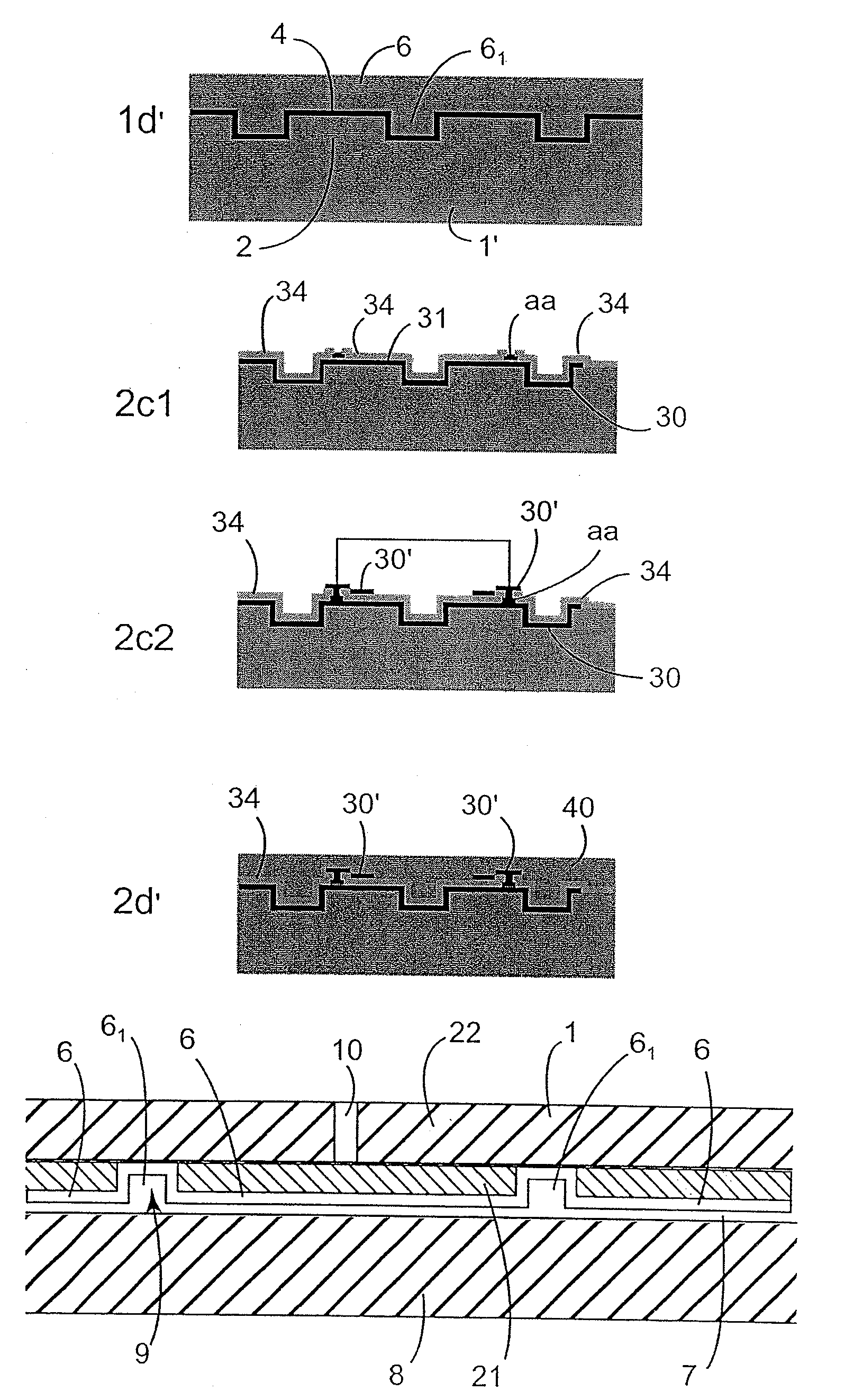
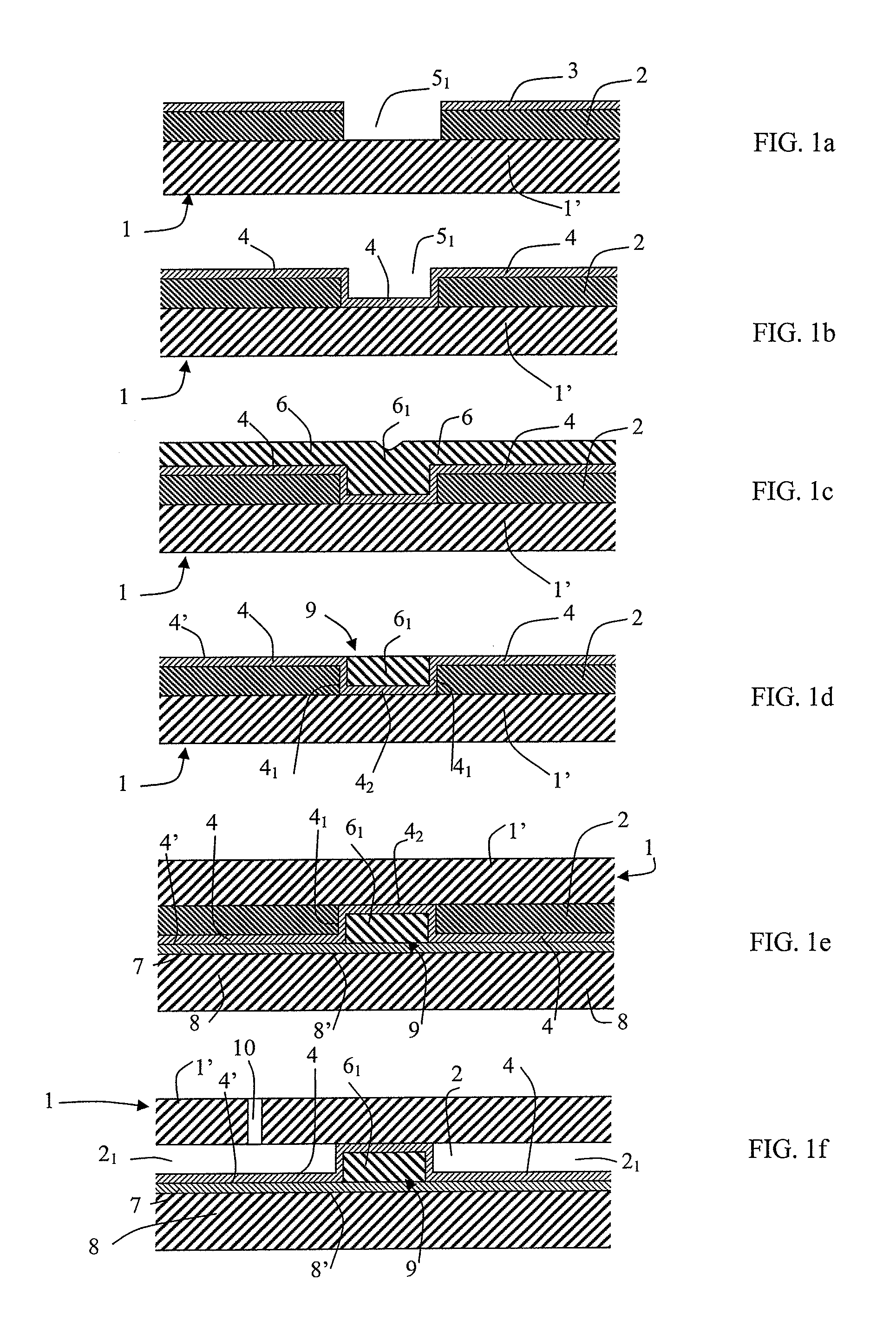
[0051]FIGS. 1a to 1f show a preferred implementation of the method of the invention, serving to enable insulating pillars to be made from wide trenches (e.g. several tens of μm and more precisely 50 μm for example). The method starts with a substrate 1 presenting at least one monocrystalline layer 1′ (e.g. of monocrystalline Si), coated in a sacrificial layer 2 (e.g. SiO2). The layer 1′ may occupy all of the substrate (thick Si substrate) or only a portion thereof (e.g. the top layer of an SOI substrate or some other type of substrate presenting an etching stop layer). Preferably, the initial substrate is a silicon substrate including a monocrystalline SiGe stop layer (not shown in the figure) and a monocrystalline silicon layer 1′. The layer 2 may be an oxide deposited by low pressure chemical vapor deposition (LPCVD) or by plasma-enhanced CVD (PECVD), or it may be made by thermally oxidizing the layer 1′. Its thickness may lie in the range 200 nanometers (nm) to 5 μm (typically in...


PUM

PropertyMeasurementUnit
thickaaaaaaaaaa
thickaaaaaaaaaa
thicknessaaaaaaaaaa

Abstract

The invention provides a method of fabricating an electromechanical structure presenting a first substrate including a layer of monocrystalline material covered in a sacrificial layer that presents a free surface, the structure presenting a mechanical reinforcing pillar in the sacrificial layer, the method including etching a well region in the sacrificial layer to define a mechanical pillar; depositing a first functionalization layer of the first material to at least partially fill the well region and cover the free surface of the sacrificial layer around the well region; depositing a second material different from the first material for terminating the filling of the well region to thereby cover the first functionalization layer around the well region, planarizing the filler layer, the pillar being formed by the superposition of the first material and second material in the well region; and releasing the electromechanical structure by removing at least partially the sacrificial layer.

Description

CROSS REFERENCE TO RELATED APPLICATIONS[0001]This application is a divisional application of application Ser. No. 12 / 488,841, filed Jun. 22, 2009, which claims priority from FR Application No. 08 03495 filed Jun. 23, 2008, the contents of which are incorporated by reference.FIELD OF THE INVENTION[0002]The present invention relates to a method of fabricating an electromechanical structure presenting a substrate of the monocrystalline layer type (being made in particular of silicon, germanium, perovskite, or quartz) on a sacrificial layer, in particular for a microsystem or a micro-electromechanical system (MEMS) or a nano-electromechanical system (NEMS), said substrate presenting at least one mechanical reinforcing region (or “pillar”).BACKGROUND OF THE INVENTION[0003]So-called surface technologies (in contrast with bulk technologies) enable the size of electromechanical structures (MEMS and / or NEMS) made on silicon to be reduced. These technologies rely on using a stack of at least ...

Claims


Application Information

Patent Timeline
Patent Type & Authority Applications(United States)
IPC IPC(8): H01L29/66
CPCH01L29/66007B81B2201/0264B81C1/00357B81C1/00682B81C2201/019H01L2924/0002H01L2924/00
Inventor LARREY, VINCENTPERRUCHOT, FRANCOISDIEM, BERNARDCLAVELIER, LAURENTROBERT, PHILIPPE
Owner COMMISSARIAT A LENERGIE ATOMIQUE ET AUX ENERGIES ALTERNATIVES
Features
  • R&D
  • Intellectual Property
  • Life Sciences
  • Materials
  • Tech Scout
  • Unparalleled Data Quality
  • Higher Quality Content
  • 60% Fewer Hallucinations
Learn More