Check patentability & draft patents in minutes with Patsnap Eureka AI!

Method of fabricating an electromechanical structure including at least one mechanical reinforcing pillar

Inactive Publication Date: 2009-12-31
COMMISSARIAT A LENERGIE ATOMIQUE ET AUX ENERGIES ALTERNATIVES
View PDF9 Cites 6 Cited by
  • Summary
  • Abstract
  • Description
  • Claims
  • Application Information

AI Technical Summary

Benefits of technology

[0012]The present invention proposes a fabrication method that enables mechanical reinforcing pillars to be fabricated in versatile manner, i.e. without limitation on their width, so their width can be a function of the intended application, and the pillars can be selected to be insulating or conductive at will, in particular in order to enable a contact to be made, while avoiding the drawback of any risk of revealing the bonding interface of a substrate on the sacrificial layer. A variant of the method makes it possible to limit the topology that stems from fabricating pillars.
[0029]It may be advantageous between steps b′) and b″) to deposit an additional layer of the first material in such a manner as to thicken the insulating first layer, in particular when the planarization of the second layer is continued until the first layer is reached.
[0034]The first functionalization layer may cover a portion only of the well region(s), the other portion of the well regions being covered by the second functionalization layer, thereby enabling the conductive pillars and insulating pillars to be formed.
[0043]Alternatively, the last interconnection level is plane and includes interconnection areas to make it possible, during assembly with the second substrate, to connect elements of the second substrate to the electromechanical structure.

Problems solved by technology

During that operation, the interface zone between the added substrate and the remainder of the structure is subjected to chemical etching (in general with HF acid), thereby leading to shapes that are poorly controlled if the interface is not perfect, since the speed of etching is variable, and there is a risk of revealing the bonding interface.
After the sacrificial layer has been removed, and the MEMS structure has been released, mechanical integrity is not good.
Nevertheless, the pillars are made of thick poly-Si and their lateral size is limited by the technology.
Known methods are therefore limited to pillars of width that is limited to the thickness of the poly-Si layer used for filling them.
Since the stress state of polycrystalline Si (at the time of deposition or during heating) is different from that of SiO2, limiting the lateral dimensions of the pillars serves to limit non-uniformities in the sacrificial layer.

Method used


Image

  • Method of fabricating an electromechanical structure including at least one mechanical reinforcing pillar
  • Method of fabricating an electromechanical structure including at least one mechanical reinforcing pillar
  • Method of fabricating an electromechanical structure including at least one mechanical reinforcing pillar

Examples


Embodiment Construction

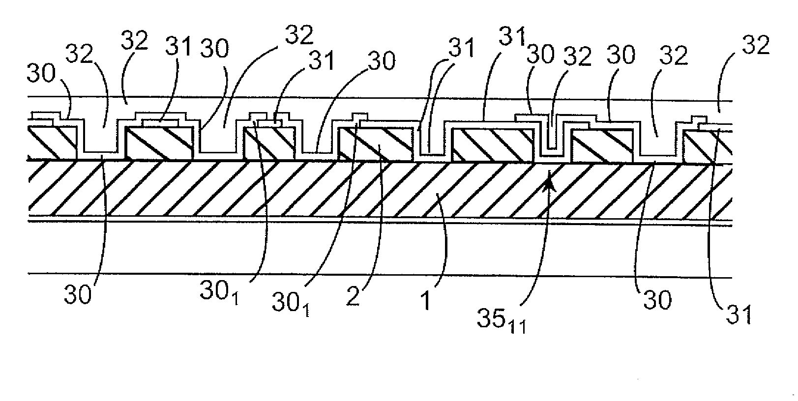
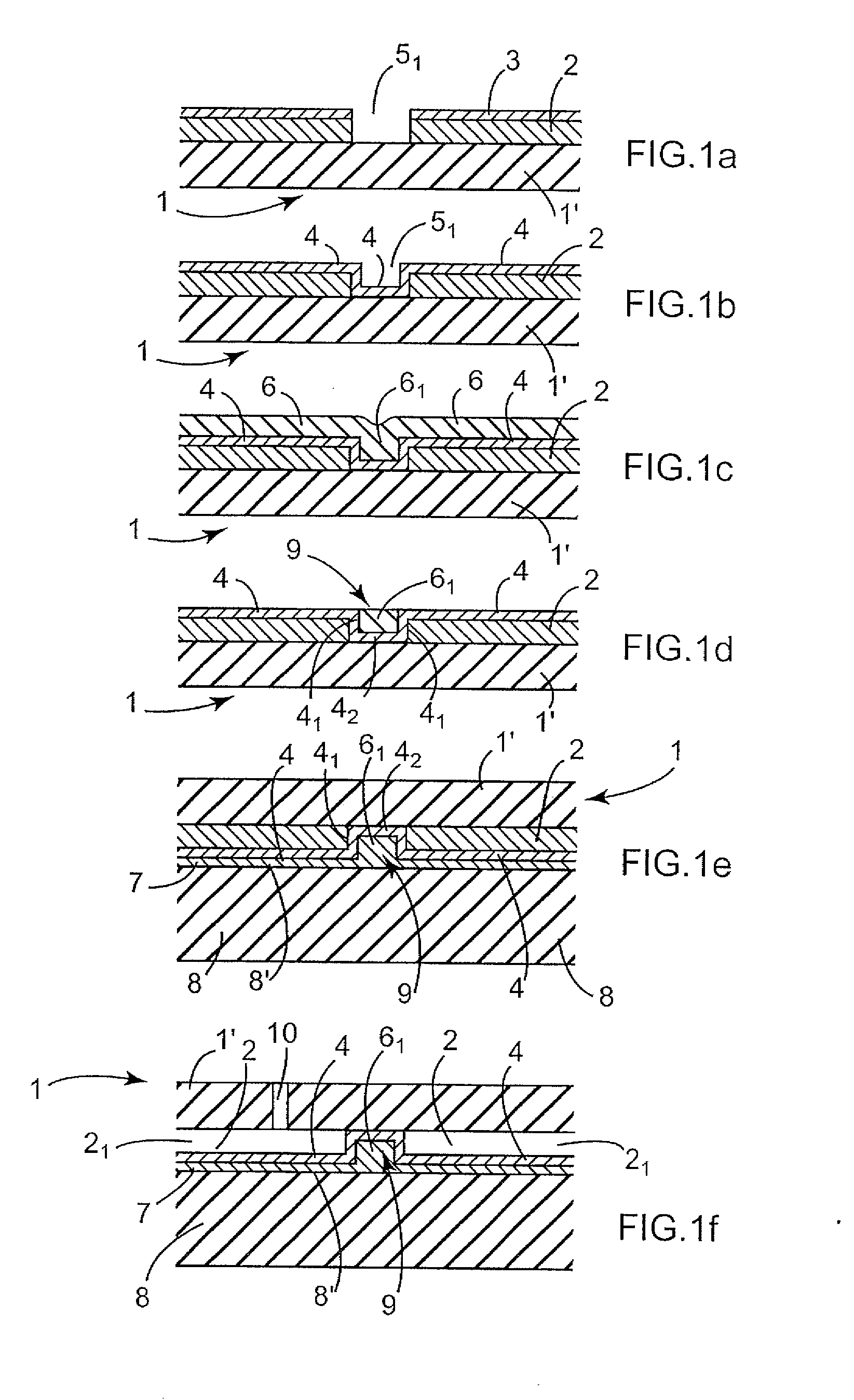
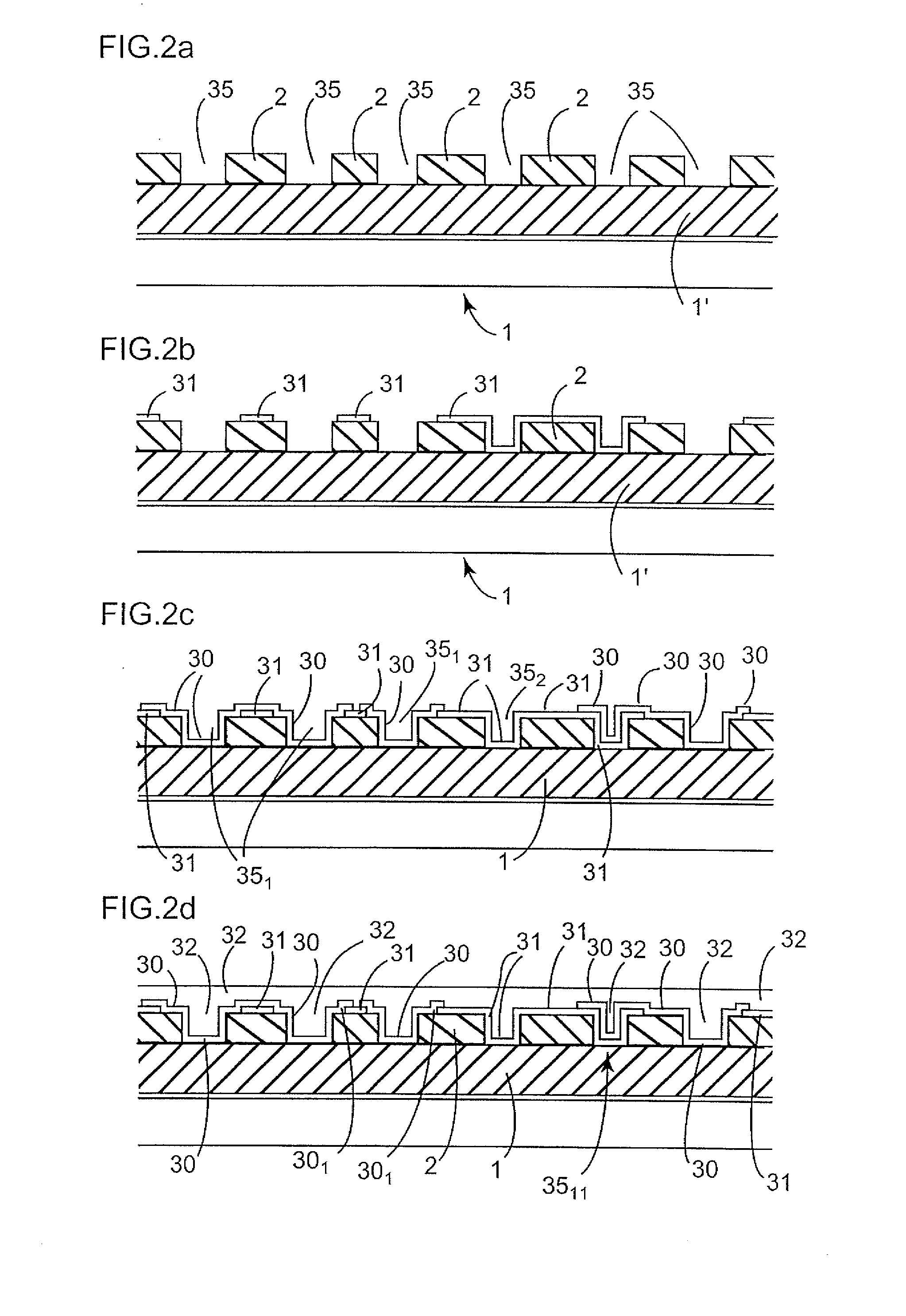
[0050]FIGS. 1a to 1f show a preferred implementation of the method of the invention, serving to enable insulating pillars to be made from wide trenches (e.g. several tens of μm and more precisely 50 μm for example). The method starts with a substrate 1 presenting at least one monocrystalline layer 1′ (e.g. of monocrystalline Si), coated in a sacrificial layer 2 (e.g. SiO2). The layer 1′ may occupy all of the substrate (thick Si substrate) or only a portion thereof (e.g. the top layer of an SOI substrate or some other type of substrate presenting an etching stop layer). Preferably, the initial substrate is a silicon substrate including a monocrystalline SiGe stop layer (not shown in the figure) and a monocrystalline silicon layer 1′. The layer 2 may be an oxide deposited by low pressure chemical vapor deposition (LPCVD) or by plasma-enhanced CVD (PECVD), or it may be made by thermally oxidizing the layer 1′. Its thickness may lie in the range 200 nanometers (nm) to 5 μm (typically in...


PUM


Abstract

The invention relates to a method of fabricating an electromechanical structure presenting a first substrate (1) including at least one layer (1′) of monocrystalline material covered in a sacrificial layer (2) that presents a free surface, the structure presenting at least one mechanical reinforcing pillar received in said sacrificial layer, the method being characterized in that it comprises:a) making at least one well region (51, 52) in the sacrificial layer (2) by etching, at least in the entire thickness of the sacrificial layer (2), the well region defining at least one said mechanical pillar;b) depositing a first functionalization layer (4, 31) of a first material, relative to which the sacrificial layer is suitable for being etched selectively, the functionalization layer (4) filling at least one well region (51) at least partially and covering the free surface of the sacrificial layer (2) at least around the well region(s); andb′) depositing a filler layer (6, 32) of a second material different from the first material for terminating the filling of the well region(s) (5′), said filler layer (6) covering the first functionalization layer (4) at least in part around the well region(s) (5′), and planarizing the filler layer (6, 32), the pillar(s) being formed by the superposition of at least the first material and the second material in the well region(s);and releasing the electromechanical structure by removing at least partially the sacrificial layer (2).The invention also relates to an electromechanical structure obtained by the method.

Description

FIELD OF THE INVENTION [0001]The present invention relates to a method of fabricating an electromechanical structure presenting a substrate of the monocrystalline layer type (being made in particular of silicon, germanium, perovskite, or quartz) on a sacrificial layer, in particular for a microsystem or a micro-electromechanical system (MEMS) or a nano-electromechanical system (NEMS), said substrate presenting at least one mechanical reinforcing region (or “pillar”).BACKGROUND OF THE INVENTION [0002]So-called surface technologies (in contrast with bulk technologies) enable the size of electromechanical structures (MEMS and / or NEMS) made on silicon to be reduced. These technologies rely on using a stack of at least three layers: a mechanical layer (typically 0.1 micrometer (μm) to 100 μm thick); a sacrificial layer (typically 0.1 μm to a few Am thick); and a support (typically 10 μm to 1000 μm thick). Selective chemical etching of the sacrificial layer makes it possible to provide fu...

Claims


Application Information

Patent Timeline
IPC IPC(8): H01L21/30H01L23/58
CPCB81B2201/0264B81C1/00357B81C1/00682B81C2201/019H01L2924/0002H01L29/66007H01L2924/00
Inventor LARREY, VINCENTPERRUCHOT, FRANCOISDIEM, BERNARDCLAVELIER, LAURENTROBERT, PHILIPPE
Owner COMMISSARIAT A LENERGIE ATOMIQUE ET AUX ENERGIES ALTERNATIVES
Features
  • R&D
  • Intellectual Property
  • Life Sciences
  • Materials
  • Tech Scout
  • Unparalleled Data Quality
  • Higher Quality Content
  • 60% Fewer Hallucinations
Learn More