Display device
a display device and display technology, applied in the direction of thermoelectric device junction materials, semiconductor devices, electrical equipment, etc., can solve the problems of increasing cost, affecting the appearance of the device,
- Summary
- Abstract
- Description
- Claims
- Application Information
AI Technical Summary
Benefits of technology
Problems solved by technology
Method used
Image
Examples
example 1
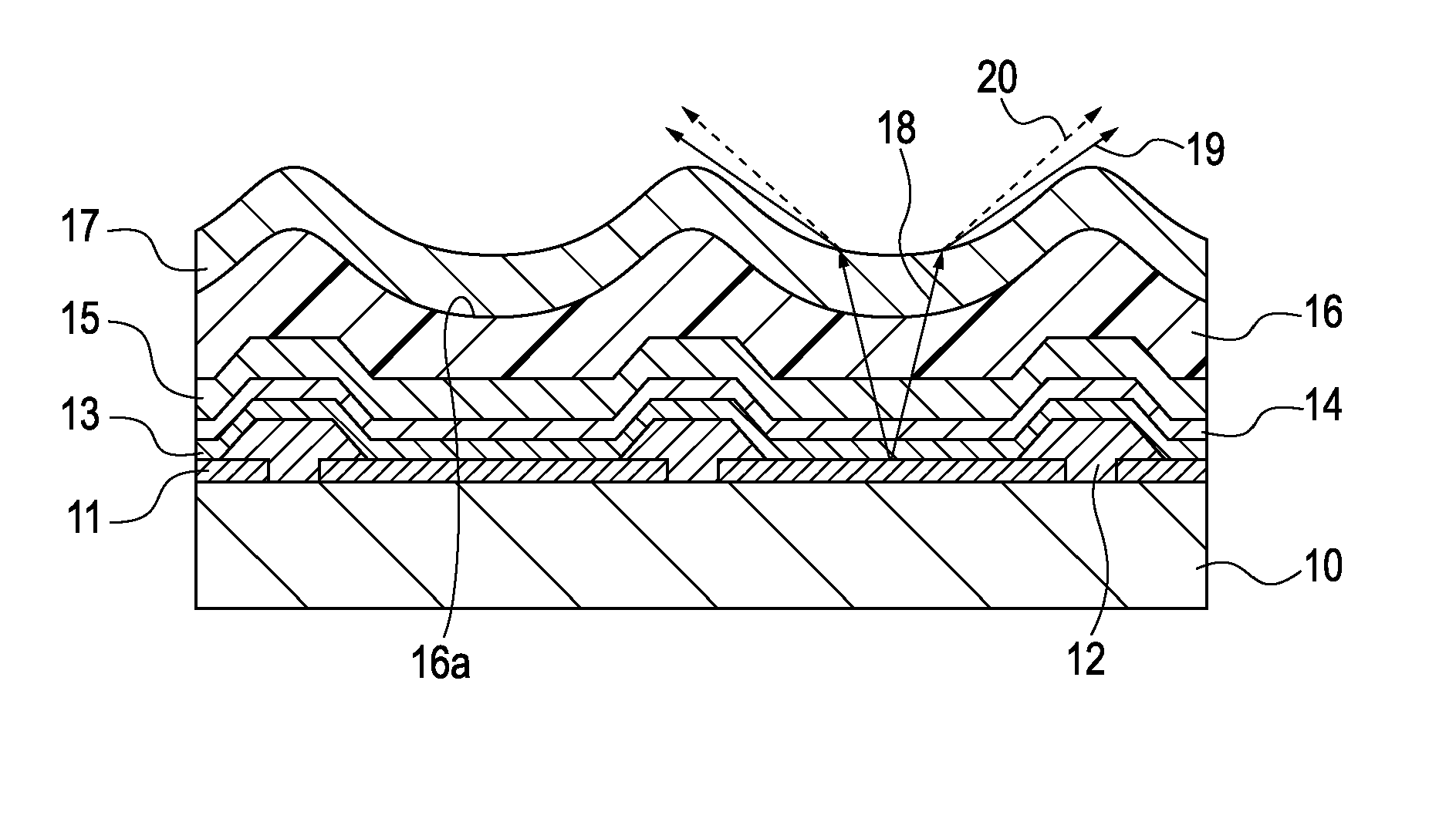
[0077]Pixel circuits (not shown) were formed on a glass substrate with low-temperature polysilicon TFTs, and an interlayer insulating layer of SiN and a planarizing layer of an acrylic resin were formed in this order on the pixel circuits to produce a board 10 shown in FIG. 4A. Then, an ITO layer and an AlNd layer were formed on the board 10 so as to respectively have thicknesses 38 nm and 100 nm by sputtering. Subsequently, the ITO layer and the AlNd layer were patterned for each pixel to form anode electrodes 11.
[0078]Then, an acrylic resin was spin coated on the anode electrodes 11 and then was patterned by lithography to form openings (these openings correspond to pixels) at the portions where the anode electrodes 11 were provided to form pixel separation layers 12. The pitch of the pixels was 30 μm, and the size of the exposed portion of each anode electrode 11 due to the opening was 10 μm. Then, ultrasonic cleaning with isopropyl alcohol (IPA), boiling cleaning, and drying wer...
example 2
[0091]A lens array was formed by a process, which is different from that of EXAMPLE 1, as shown in FIGS. 6A to 6E. Incidentally, since the steps until the first protective layer 15 is formed are the same as those in EXAMPLE 1, the descriptions thereof are omitted, and the description will be started from the step of forming the second protective layer 16.
[0092]First, a thermosetting epoxy resin (second protective layer 16 of a thermosetting resin material) with a viscosity of 3000 mPa·s was applied on the first protective layer 15 at a thickness of 10 μm with a dispenser (SHOT MINI SL: a product of Musashi Engineering, Inc.), which enables precise drawing, under a nitrogen atmosphere at a dew-point temperature of 60° C. (FIG. 6A). Then, the epoxy resin was cured by heating at 100° C. for 15 minutes under a vacuum environment.
[0093]Subsequently, the same resin 23 was applied on the second protective layer 16 at a thickness of 4 μm (FIG. 6B) and was exposed from above with a photomask...
PUM
 Abstract
Description
Claims
Application Information
 - Generate Ideas
- Intellectual Property
- Life Sciences
- Materials
- Tech Scout
- Unparalleled Data Quality
- Higher Quality Content
- 60% Fewer Hallucinations
Browse by: Latest US Patents, China's latest patents, Technical Efficacy Thesaurus, Application Domain, Technology Topic, Popular Technical Reports.
© 2025 PatSnap. All rights reserved.Legal|Privacy policy|Modern Slavery Act Transparency Statement|Sitemap|About US| Contact US: help@patsnap.com


